BSO604NS2 OptiMOS Power-Transistor
Feature
• Dual N-Channel
Product Summary VDS R DS(on) ID 55 35 5
P-DSO-8 -7
V mΩ A...
BSO604NS2 OptiMOS Power-Transistor
Feature
Dual N-Channel
Product Summary VDS R DS(on) ID 55 35 5
P-DSO-8 -7
V mΩ A
Enhancement mode Logic Level 150 °C operating temperature Avalanche rated dv/dt rated
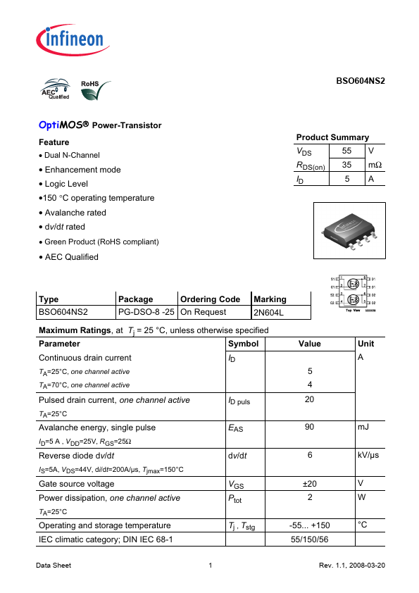
Type BSO604NS2
Package P-DSO-8 -7
Ordering Code Q67060-S7309
Marking 2N604L
Maximum Ratings, at Tj = 25 °C, unless otherwise specified Parameter Continuous drain current
TA=25°C, one channel active TA=70°C, one channel active
Symbol ID
Value 5 4
Unit A
Pulsed drain current, one channel active
TA=25°C
ID puls EAS dv/dt VGS Ptot Tj , Tstg
20 90 6 ±20 2 -55... +150 55/150/56 mJ kV/µs V W °C
Avalanche energy, single pulse
ID=5 A , VDD=25V, RGS=25Ω
Reverse diode dv/dt
IS=5A, VDS=44V, di/dt=200A/µs, Tjmax=150°C
Gate source
voltage Power dissipation, one channel active
TA=25°C
Operating and storage temperature IEC climatic category; DIN IEC 68-1
Page 1
2003-10-28
BSO604NS2
Thermal Characteristics Parameter Characteristics Thermal resistance, junction - soldering point SMD version, device on PCB:
@ min. footprint ; t ≤ 10 s @ 6 cm2 cooling area 1) ; t ≤10 s
Symbol min.
RthJS RthJA
Values typ. 34 max. 50 100 62.5
Unit
-
K/W
Electrical Characteristics , at Tj = 25 °C, unless otherwise specified Parameter Static Characteristics Drain-source breakdown
voltage
V GS=0V, I D=1mA
Symbol min. V(BR)DSS VGS(th) IDSS IGSS RDS(on) RDS(on) 55 1.2
Values typ. 1.6 max. 2
Unit
V
Gate threshold
voltage, VGS = VDS
ID=30µA
Zero gate
voltage drain current
V DS=5...