Philips Semiconductors
Product specification
N-channel enhancement mode TrenchMOS™ transistor
FEATURES
• ’Trench’ tech...
Philips Semiconductors
Product specification
N-channel enhancement mode TrenchMOS™ transistor
FEATURES
’Trench’ technology Low on-state resistance Fast switching High thermal cycling performance Low thermal resistance
BSP100
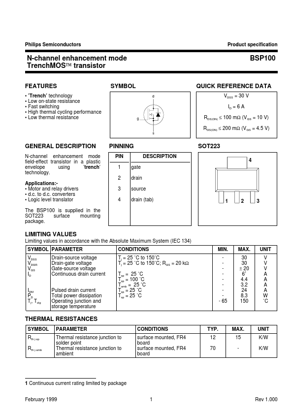
SYMBOL
d
QUICK REFERENCE DATA
VDSS = 30 V ID = 6 A
g
RDS(ON) ≤ 100 mΩ (VGS = 10 V) RDS(ON) ≤ 200 mΩ (VGS = 4.5 V)
s
GENERAL DESCRIPTION
N-channel enhancement mode field-effect transistor in a plastic envelope using ’trench’ technology. Applications: Motor and relay drivers d.c. to d.c. converters Logic level translator The BSP100 is supplied in the SOT223 surface mounting package.
PINNING
PIN 1 2 3 4 gate drain source drain (tab) DESCRIPTION
SOT223
4
1
2
3
LIMITING VALUES
Limiting values in accordance with the Absolute Maximum System (IEC 134) SYMBOL PARAMETER VDSS VDGR VGS ID IDM PD Tj, Tstg Drain-source
voltage Drain-gate
voltage Gate-source
voltage Continuous drain current Pulsed drain current Total power dissipation Operating junction and storage temperature CONDITIONS Tj = 25 ˚C to 150˚C Tj = 25 ˚C to 150˚C; RGS = 20 kΩ Tsp = 25 ˚C Tsp = 100 ˚C Tamb = 25 ˚C Tsp = 25 ˚C Tsp = 25 ˚C MIN. - 65 MAX. 30 30 ± 20 61 4.4 3.2 24 8.3 150 UNIT V V V A A A A W ˚C
THERMAL RESISTANCES
SYMBOL Rth j-sp Rth j-amb PARAMETER Thermal resistance junction to solder point Thermal resistance junction to ambient CONDITIONS surface mounted, FR4 board surface mounted, FR4 board TYP. 12 70 MAX. 15 UNIT K/W K/W
1 Continuous current rating limited by...