BSP16T1G
High Voltage Transistors
PNP Silicon
Features
These Devices are Pb--Free, Halogen Free/BFR Free and are RoHS...
BSP16T1G
High
Voltage Transistors
PNP Silicon
Features
These Devices are Pb--Free, Halogen Free/BFR Free and are RoHS
Compliant
MAXIMUM RATINGS
Rating
Symbol
Value
Unit
Collector-Emitter
Voltage Collector-Base
Voltage Emitter-Base
Voltage Collector Current Total Device Dissipation @ TA = 25C
(Note 1)
VCEO VCBO VEBO
IC PD
--300 --350 --6.0 --100 1.5
Vdc Vdc Vdc mAdc W
Storage Temperature Range
PD
--65 to
C
+150
Junction Temperature
TJ 150 C
THERMAL CHARACTERISTICS
Characteristic
Symbol
Max
Unit
Thermal Resistance, Junction--to--Ambient
RθJA
83.3 C/W
Stresses exceeding Maximum Ratings may damage the device. Maximum Ratings are stress ratings only. Functional operation above the Recommended Operating Conditions is not implied. Extended exposure to stresses above the Recommended Operating Conditions may affect device reliability. 1. Device mounted on a glass epoxy printed circuit board 1.575 in x 1.575 in x
0.059 in; mounting pad for the collector lead min. 0.93 sq. in.
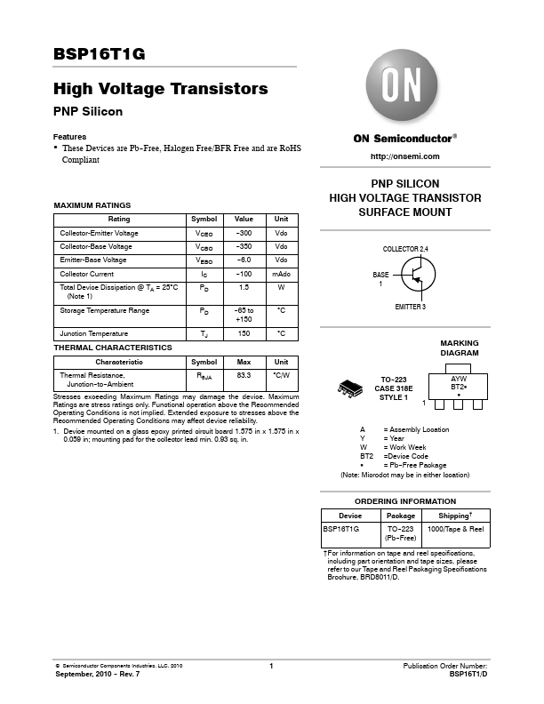
http://onsemi.com
PNP SILICON HIGH
VOLTAGE TRANSISTOR
SURFACE MOUNT
COLLECTOR 2,4
BASE 1
EMITTER 3
MARKING DIAGRAM
TO--223 CASE 318E
STYLE 1
1
AYW BT2G
G
A = Assembly Location Y = Year W = Work Week BT2 =Device Code G = Pb--Free Package
(Note: Microdot may be in either location)
ORDERING INFORMATION
Device
Package
Shipping†
BSP16T1G
TO--223 1000/Tape & Reel (Pb--Free)
†For information on tape and reel specifications, including part orientation and tape sizes, please re...