SIPMOS Power Transistor (P-Channel Enhancement mode Avalanche rated Logic Level dv/dt rated)
BSP 171 P
Preliminary data SIPMOS® Power Transistor • P-Channel
• Enhancement
mode
• Avalanche rated • Logic Level • d...
BSP 171 P
Preliminary data SIPMOS® Power Transistor P-Channel
Enhancement
mode
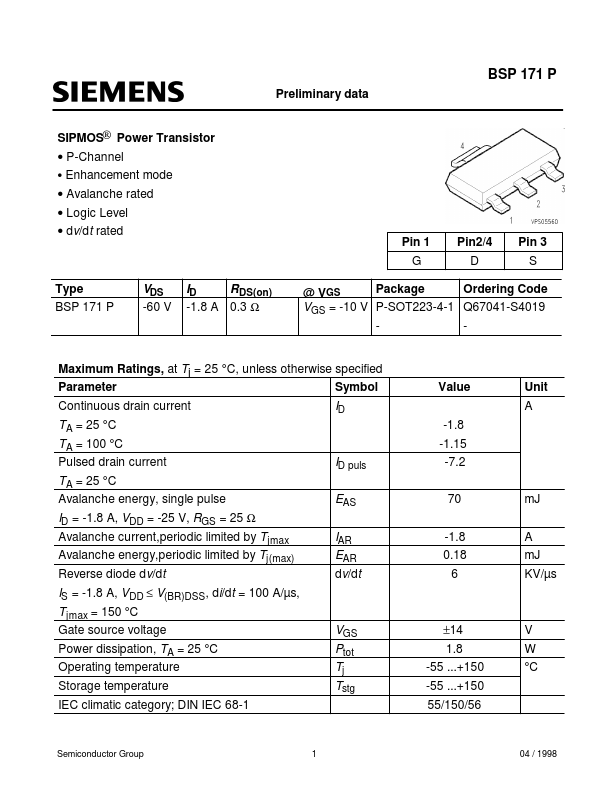
Avalanche rated Logic Level dv/dt rated Pin 1 G Type BSP 171 P VDS -60 V ID RDS(on) Pin2/4 D Pin 3 S
-1.8 A 0.3 Ω
Package Ordering Code @ VGS VGS = -10 V P-SOT223-4-1 Q67041-S4019 -
Maximum Ratings, at Tj = 25 °C, unless otherwise specified Parameter Symbol Continuous drain current T A = 25 °C T A = 100 °C Pulsed drain current T A = 25 °C Avalanche energy, single pulse ID = -1.8 A, VDD = -25 V, RGS = 25 Ω Avalanche current,periodic limited by Tjmax Avalanche energy,periodic limited by Tj(max) Reverse diode dv/dt IS = -1.8 A, V DD ≤V(BR)DSS, di/dt = 100 A/µs, T jmax = 150 °C Gate source
voltage Power dissipation, TA = 25 °C Operating temperature Storage temperature IEC climatic category; DIN IEC 68-1 VGS Ptot Tj Tstg IAR EAR dv/dt EAS ID puls ID
Value -1.8 -1.15 -7.2 70 -1.8 0.18 6
Unit A
mJ A mJ KV/µs
±14 1.8 -55 ...+150 -55 ...+150 55/150/56
V W °C
Semiconductor Group
1
04 / 1998
BSP 171 P
Preliminary data Electrical Characteristics Parameter at Tj = 25 °C, unless otherwise specified Thermal Characteristics Thermal resistance, junction -soldering point (Pin 4) Thermal resistance, junction - ambient SMD version, device on PCB: @ min. footprint @ 6 cm2 cooling areaF) RthJS RthJA RthJA tbd tbd 70 Symbol min. Values typ. tbd max. tbd K/W Unit
Static Characteristics Drain- source breakdown
voltage VGS = 0 V, ID = -0.25 mA Gate threshold
voltage, VGS = VDS ID = -460 µA, Tj = 25 ...