BSP 296
SIPMOS ® Small-Signal Transistor • N channel • Enhancement mode • Logic Level
• VGS(th) = 0.8...2.0V
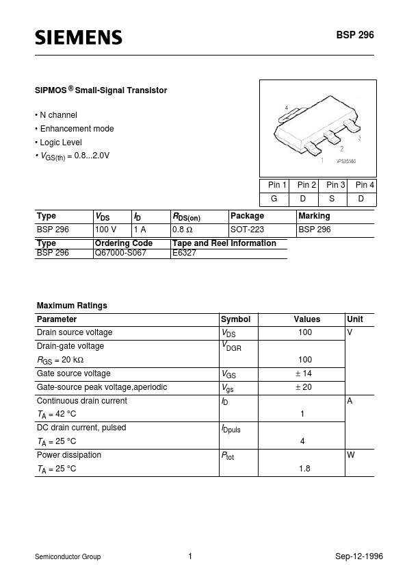
Pin 1 G T...
BSP 296
SIPMOS ® Small-Signal Transistor N channel Enhancement mode Logic Level
VGS(th) = 0.8...2.0V
Pin 1 G Type BSP 296 Type BSP 296 Pin 2 D Pin 3 S Pin 4 D
VDS
100 V
ID
1A
RDS(on)
0.8 Ω
Package SOT-223
Marking BSP 296
Ordering Code Q67000-S067
Tape and Reel Information E6327
Maximum Ratings Parameter Drain source
voltage Drain-gate
voltage Symbol Values 100 100 Unit V
VDS VDGR VGS Vgs ID
RGS = 20 kΩ
Gate source
voltage Gate-source peak
voltage,aperiodic Continuous drain current
± 14 ± 20 A 1
TA = 42 °C
DC drain current, pulsed
IDpuls
4
TA = 25 °C
Power dissipation
Ptot
1.8
W
TA = 25 °C
Semiconductor Group
1
Sep-12-1996
BSP 296
Maximum Ratings Parameter Chip or operating temperature Storage temperature Thermal resistance, chip to ambient air Therminal resistance, junction-soldering point 1) DIN humidity category, DIN 40 040 IEC climatic category, DIN IEC 68-1 Symbol Values -55 ... + 150 -55 ... + 150 ≤ 70 ≤ 10 E 55 / 150 / 56 K/W Unit °C
Tj Tstg RthJA RthJS
1) Transistor on epoxy pcb 40 mm x 40 mm x 1,5 mm with 6 cm2 copper area for drain connection
Electrical Characteristics, at Tj = 25°C, unless otherwise specified Parameter Symbol min. Static Characteristics Drain- source breakdown
voltage Values typ. max. Unit
V(BR)DSS
100 1.4 0.1 8 10 0.55 0.95 2 1 50 100 100
V
VGS = 0 V, ID = 0.25 mA, Tj = 25 °C
Gate threshold
voltage
VGS(th)
0.8
VGS=VDS, ID = 1 mA
Zero gate
voltage drain current
IDSS
µA nA nA Ω 0.8 1.4
VDS = 100 V, VGS = 0 V,...