BSS 88
SIPMOS ® Small-Signal Transistor • N channel • Enhancement mode • Logic Level
• VGS(th) = 0.8...2.0V
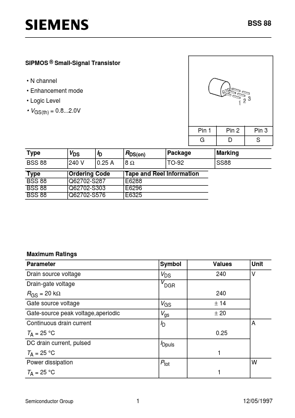
Pin 1 G Ty...
BSS 88
SIPMOS ® Small-Signal Transistor N channel Enhancement mode Logic Level
VGS(th) = 0.8...2.0V
Pin 1 G Type BSS 88 Type BSS 88 BSS 88 BSS 88 Pin 2 D Marking SS88 Pin 3 S
VDS
240 V
ID
0.25 A
RDS(on)
8Ω
Package TO-92
Ordering Code Q62702-S287 Q62702-S303 Q62702-S576
Tape and Reel Information E6288 E6296 E6325
Maximum Ratings Parameter Drain source
voltage Drain-gate
voltage Symbol Values 240 240 Unit V
VDS V
DGR
RGS = 20 kΩ
Gate source
voltage Gate-source peak
voltage,aperiodic Continuous drain current
VGS Vgs ID
± 14 ± 20 A 0.25
TA = 25 °C
DC drain current, pulsed
IDpuls
1
TA = 25 °C
Power dissipation
Ptot
1
W
TA = 25 °C
Semiconductor Group
1
12/05/1997
BSS 88
Maximum Ratings Parameter Chip or operating temperature Storage temperature Thermal resistance, chip to ambient air 1) DIN humidity category, DIN 40 040 IEC climatic category, DIN IEC 68-1 Symbol Values -55 ... + 150 -55 ... + 150 ≤ 125 E 55 / 150 / 56 K/W Unit °C
Tj Tstg RthJA
Electrical Characteristics, at Tj = 25°C, unless otherwise specified Parameter Symbol min. Values typ. max. Unit
Static Characteristics Drain- source breakdown
voltage
V(BR)DSS
240 0.8 0.1 10 10 5 7 1.2 1 100 100 100
V
VGS = 0 V, ID = 0.25 mA, Tj = 25 °C
Gate threshold
voltage
VGS(th)
0.6
VGS=VDS, ID = 1 mA
Zero gate
voltage drain current
IDSS
µA nA nA Ω 8 15
VDS = 240 V, VGS = 0 V, Tj = 25 °C VDS = 240 V, VGS = 0 V, Tj = 125 °C VDS = 100 V, VGS = 0 V, Tj = 25 °C
Gate-source leakage current
IGSS RDS...