SOT23 N CHANNEL ENHANCEMENT MODE VERTICAL DMOS FET I
I Issue 2 - October 1997 PARTMARKING DETAIL – O2
www.DataSheet4U.c...
SOT23 N CHANNEL ENHANCEMENT MODE VERTICAL DMOS FET I
I Issue 2 - October 1997 PARTMARKING DETAIL – O2
www.DataSheet4U.com
BST82
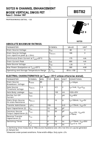
C B
E
SOT23
ABSOLUTE MAXIMUM RATINGS.
PARAMETER Drain Source
Voltage Drain Source
Voltage (non repetitive peak tp ≤ 2ms) Continuous Drain Current at T amb=25°C Drain Current Peak Gate-Source
Voltage Max Power Dissipation at T amb=25°C Operating and Storage Temperature Range SYMBOL V DS V DS(sm) ID I DM V GS PD T j :T stg VALUE 80 100 175 600 ± 20 300 -55 to +150 UNIT V V mA mA V mW °C
ELECTRIAL CHARACTERISTICS (at Tamb = 25°C unless otherwise stated).
PARAMETER Drain Source Breakdown
Voltage Gate Source Threshold
Voltage Gate Body Leakage Emitter Cut-Off Current Static Drain-Source On-state Resistance Transfer Admittance Input Capacitance (2) SYMBOL B VDSS V GS(th) I GSS I DSS R DS(on) | yfs | C iss 7 150 15 13 3 4 4 30 20 6 10 10 MIN. 80 1.5 3.5 100 1 10 TYP. MAX. UNIT V V nA µA Ω mS pF pF pF ns ns I D=175mA, V DD=50V V GS=0 to 10V V DS=10V, V GS=0V f=1MHz CONDITIONS. I C=100 µ A I D=1mA, V DS=V GS VGS=20V V DS=60V I D=150mA, V GS=5V I D=175mA, V DS=5V
Common Source C oss Output Capacitance (2) Reverse Transfer Capacitance (2) Switching Times C rss T on T off
(1) Swithcing times measured at 150Ω source impedance and <5ns rise time on a pulse generator (2) Sample test *Measured under pulsed conditions. Pulse width=300µs. Duty cycle ≤ 2%
...