Standard ICs
Quad 2-input AND gate
BU4081B / BU4081BF / BU4081BFV
The BU4081B, BU4081BF, and BU4081BFV are dual-input p...
Standard ICs
Quad 2-input AND gate
BU4081B / BU4081BF / BU4081BFV
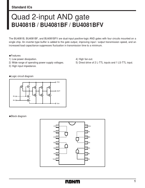
The BU4081B, BU4081BF, and BU4081BFV are dual-input positive-logic AND gates with four circuits mounted on a single chip. An inverter-type buffer is added to the gate output, improving input / output transmission speed, and an increased load capacitance suppresses fluctuation in transmission time to a minimum.
Features 1) Low power dissipation. 2) Wide range of operating power supply
voltages. 3) High input impedance.
4) High fan-out. 5) Direct drive of 2 L-TTL inputs and 1 LS-TTL input.
Logic circuit diagram
VDD OUT IN IN VSS
Block diagram
A1 1 14 VDD 13 A4 12 B4 11 O4 10 O3 9 B1 2
O1
3
O2
4
B2
5
A2
6
B3
VSS
7
8
A3
1
Standard ICs
BU4081B / BU4081BF / BU4081BFV
SS
Absolute maximum ratings (Ta = 25°C,V
Parameter Power supply
voltage Power dissipation Operating temperature Storage temperature Input
voltage I / O pin current Symbol VDD Pd Topr Tstg VIN II / O
= 0V )
Limits – 0.3 ~ + 18 1000 (DIP), 450 (SOP), 350 (SSOP) – 40 ~ + 85 – 55 ~ + 150 – 0.3 ~ VDD + 0.3 ± 10 Unit V mW °C °C V mA
Electrical characteristics (unless otherwise noted, V
Parameter Symbol Min. 3.5 Input high level
voltage VIH 7.0 11.0 — Input low level
voltage VIL — — Input high level current Input low level current IIH IIL — — 4.95 Output high level
voltage VOH 9.95 14.95 — Output low level
voltage VOL — — – 0.16 Output high level current IOH – 0.4 – 1.2 0.44 Output low level current IOL 1.1 3.0 — Static current dis...