Philips Semiconductors
PowerMOS transistor
Product Specification
BUK445-60A/B
GENERAL DESCRIPTION
N-channel enhancemen...
Philips Semiconductors
PowerMOS transistor
Product Specification
BUK445-60A/B
GENERAL DESCRIPTION
N-channel enhancement mode field-effect power transistor in a plastic full-pack envelope. The device is intended for use in Switched Mode Power Supplies (SMPS), motor control, welding, DC/DC and AC/DC converters, and in automotive and general purpose switching applications.
QUICK REFERENCE DATA
SYMBOL PARAMETER
VDS ID Ptot Tj RDS(ON)
BUK445 Drain-source
voltage Drain current (DC) Total power dissipation Junction temperature Drain-source on-state resistance
MAX.
-60A 60 21 30 150
0.038
MAX.
-60B 60 20 30 150
0.045
UNIT
V A W ˚C Ω
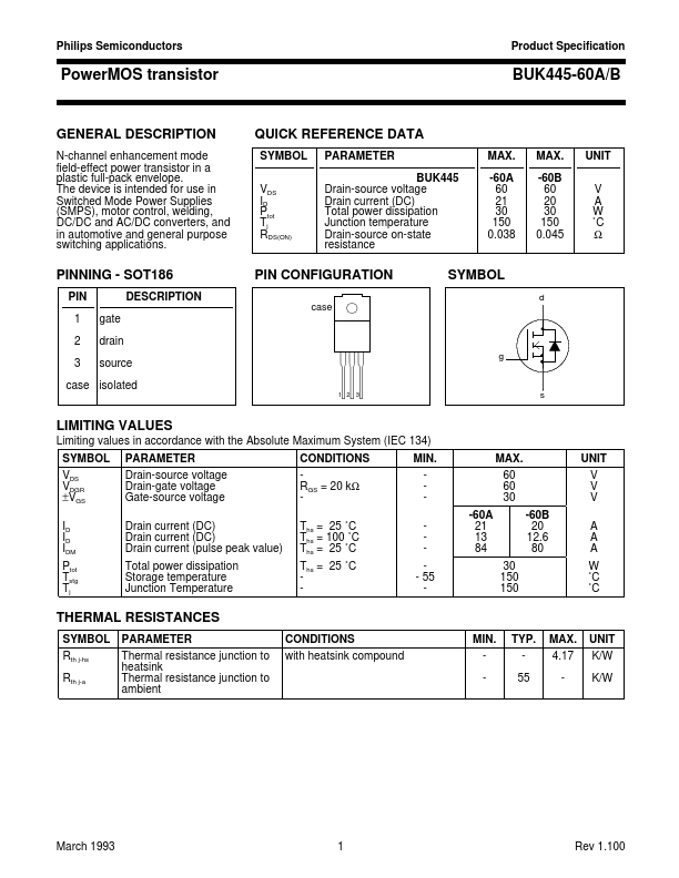
PINNING - SOT186
PIN
DESCRIPTION
1 gate
2 drain
3 source
case isolated
PIN CONFIGURATION
case
12 3
SYMBOL
d
g s
LIMITING VALUES
Limiting values in accordance with the Absolute Maximum System (IEC 134)
SYMBOL PARAMETER
CONDITIONS
MIN.
VDS VDGR ±VGS
Drain-source
voltage Drain-gate
voltage Gate-source
voltage
-
-
RGS = 20 kΩ
-
-
-
ID
Drain current (DC)
Ths = 25 ˚C
-
ID
Drain current (DC)
Ths = 100 ˚C
-
IDM
Drain current (pulse peak value) Ths = 25 ˚C
-
Ptot
Total power dissipation
Tstg
Storage temperature
Tj
Junction Temperature
Ths = 25 ˚C
-
-
- 55
-
-
THERMAL RESISTANCES
SYMBOL Rth j-hs Rth j-a
PARAMETER
Thermal resistance junction to heatsink Thermal resistance junction to ambient
CONDITIONS with heatsink compound
MAX.
60 60 30
-60A 21 13 84
-60B 20 12.6 80
30 150 150
UNIT
V V V
A A A
W ˚C ˚C...