Philips Semiconductors
Product Specification
PowerMOS transistor Logic level FET
GENERAL DESCRIPTION
N-channel enhance...
Philips Semiconductors
Product Specification
PowerMOS transistor Logic level FET
GENERAL DESCRIPTION
N-channel enhancement mode logic level field-effect power transistor in a plastic envelope. The device is intended for use in Switched Mode Power Supplies (SMPS), motor control, welding, DC/DC and AC/DC converters, and in automotive and general purpose switching applications.
BUK553-60A/B
QUICK REFERENCE DATA
SYMBOL VDS ID Ptot Tj RDS(ON) PARAMETER BUK553 Drain-source
voltage Drain current (DC) Total power dissipation Junction temperature Drain-source on-state resistance; VGS = 5 V MAX. -60A 60 21 75 175 0.085 MAX. -60B 60 20 75 175 0.10 UNIT V A W ˚C Ω
PINNING - TO220AB
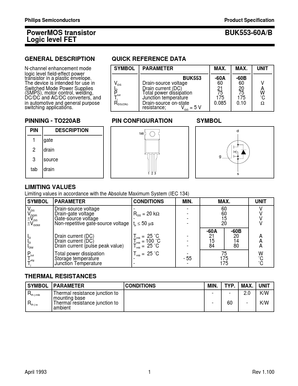
PIN 1 2 3 tab gate drain source drain DESCRIPTION
PIN CONFIGURATION
tab
SYMBOL
d
g
1 23
s
LIMITING VALUES
Limiting values in accordance with the Absolute Maximum System (IEC 134) SYMBOL VDS VDGR ±VGS ±VGSM ID ID IDM Ptot Tstg Tj PARAMETER Drain-source
voltage Drain-gate
voltage Gate-source
voltage Non-repetitive gate-source
voltage Drain current (DC) Drain current (DC) Drain current (pulse peak value) Total power dissipation Storage temperature Junction Temperature CONDITIONS RGS = 20 kΩ tp ≤ 50 µs Tmb = 25 ˚C Tmb = 100 ˚C Tmb = 25 ˚C Tmb = 25 ˚C MIN. - 55 -60A 21 15 84 75 175 175 MAX. 60 60 15 20 -60B 20 14 80 UNIT V V V V A A A W ˚C ˚C
THERMAL RESISTANCES
SYMBOL Rth j-mb Rth j-a PARAMETER Thermal resistance junction to mounting base Thermal resistance junction to ambient CONDITIONS MIN. TYP. 60 M...