Philips Semiconductors
Product Specification
PowerMOS transistor Logic level FET
GENERAL DESCRIPTION
N-channel enhance...
Philips Semiconductors
Product Specification
PowerMOS transistor Logic level FET
GENERAL DESCRIPTION
N-channel enhancement mode logic level field-effect power transistor in a plastic envelope suitable for surface mount applications. The device is intended for use in automotive and general purpose switching applications.
BUK581-60A
QUICK REFERENCE DATA
SYMBOL VDS ID Ptot Tj RDS(ON) PARAMETER Drain-source
voltage Drain current (DC) Total power dissipation Junction temperature Drain-source on-state resistance; VGS = 5 V MAX. 60 1.5 1.5 150 0.40 UNIT V A W ˚C Ω
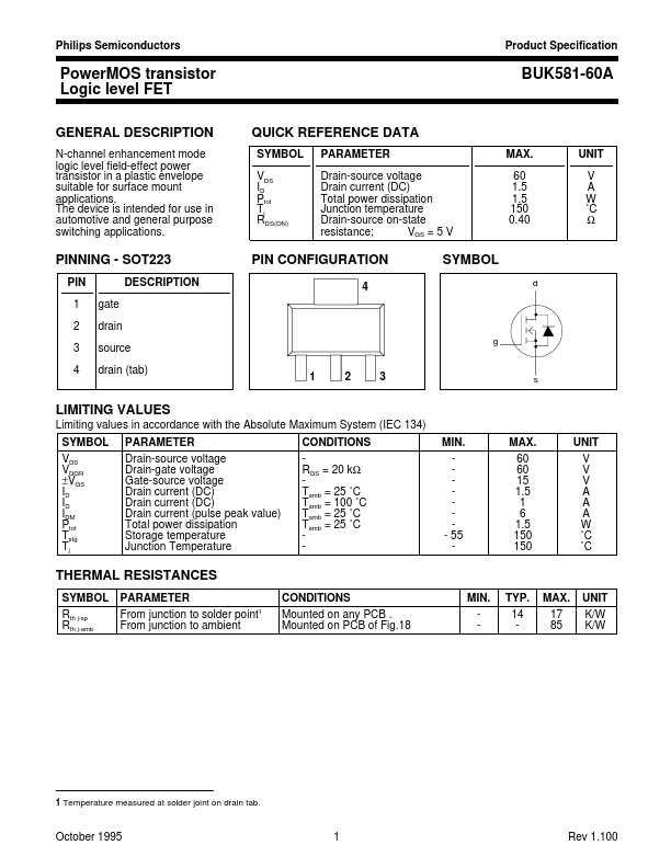
PINNING - SOT223
PIN 1 2 3 4 gate drain source drain (tab) DESCRIPTION
PIN CONFIGURATION
4
SYMBOL
d
g
1
2
3
s
LIMITING VALUES
Limiting values in accordance with the Absolute Maximum System (IEC 134) SYMBOL VDS VDGR ±VGS ID ID IDM Ptot Tstg Tj PARAMETER Drain-source
voltage Drain-gate
voltage Gate-source
voltage Drain current (DC) Drain current (DC) Drain current (pulse peak value) Total power dissipation Storage temperature Junction Temperature CONDITIONS RGS = 20 kΩ Tamb = 25 ˚C Tamb = 100 ˚C Tamb = 25 ˚C Tamb = 25 ˚C MIN. - 55 MAX. 60 60 15 1.5 1 6 1.5 150 150 UNIT V V V A A A W ˚C ˚C
THERMAL RESISTANCES
SYMBOL Rth j-sp Rth j-amb PARAMETER From junction to solder point From junction to ambient
1
CONDITIONS Mounted on any PCB . Mounted on PCB of Fig.18
MIN. -
TYP. 14 -
MAX. 17 85
UNIT K/W K/W
1 Temperature measured at solder joint on drain tab.
October 1995
1
Rev 1.100
Philips Semiconductors
Produ...