®
BUL118
HIGH VOLTAGE FAST-SWITCHING NPN POWER TRANSISTOR
s s s s
s
NPN TRANSISTOR HIGH VOLTAGE CAPABILITY LOW SPREA...
®
BUL118
HIGH
VOLTAGE FAST-SWITCHING NPN POWER TRANSISTOR
s s s s
s
NPN TRANSISTOR HIGH
VOLTAGE CAPABILITY LOW SPREAD OF DYNAMIC PARAMETERS MINIMUM LOT-TO-LOT SPREAD FOR RELIABLE OPERATION VERY HIGH SWITCHING SPEED
APPLICATIONS: s ELECTRONIC BALLASTS FOR FLUORESCENT LIGHTING DESCRIPTION The device is manufactured using high
voltage Multi Epitaxial Planar technology for high switching speeds and medium
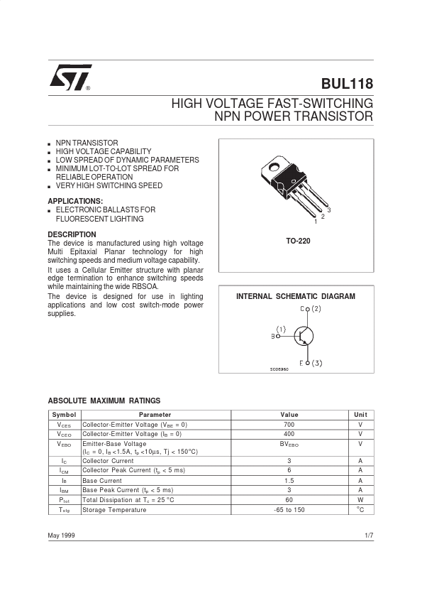
voltage capability. It uses a Cellular Emitter structure with planar edge termination to enhance switching speeds while maintaining the wide RBSOA. The device is designed for use in lighting applications and low cost switch-mode power supplies. TO-220
3 1 2
INTERNAL SCHEMATIC DIAGRAM
ABSOLUTE MAXIMUM RATINGS
Symbol V CES V CEO V EBO IC I CM IB I BM P t ot T stg Parameter Collector-Emitter
Voltage (V BE = 0) Collector-Emitter
Voltage (IB = 0) Emitter-Base
Voltage o (I C = 0, I B <1.5A, tp <10 µ s, Tj < 150 C) Collector Current Collector Peak Current (tp < 5 ms) Base Current Base Peak Current (tp < 5 ms) Total Dissipation at Tc = 25 C St orage Temperature
o
Value 700 400 BV EBO 3 6 1.5 3 60 -65 to 150
Uni t V V V A A A A W
o
C
May 1999
1/7
BUL118
THERMAL DATA
R t hj-ca se R t hj- amb Thermal Resistance Junction-Case Thermal Resistance Junction-Ambient Max Max 2.08 62.5
o o
C/W C/W
ELECTRICAL CHARACTERISTICS (Tcase = 25 oC unless otherwise specified)
Symb ol I CES BV EBO Parameter Collector Cut-off Current (V BE = -1.5 V) Emitter-Base Breakdown
Voltage (I C =0) Coll...