LAB
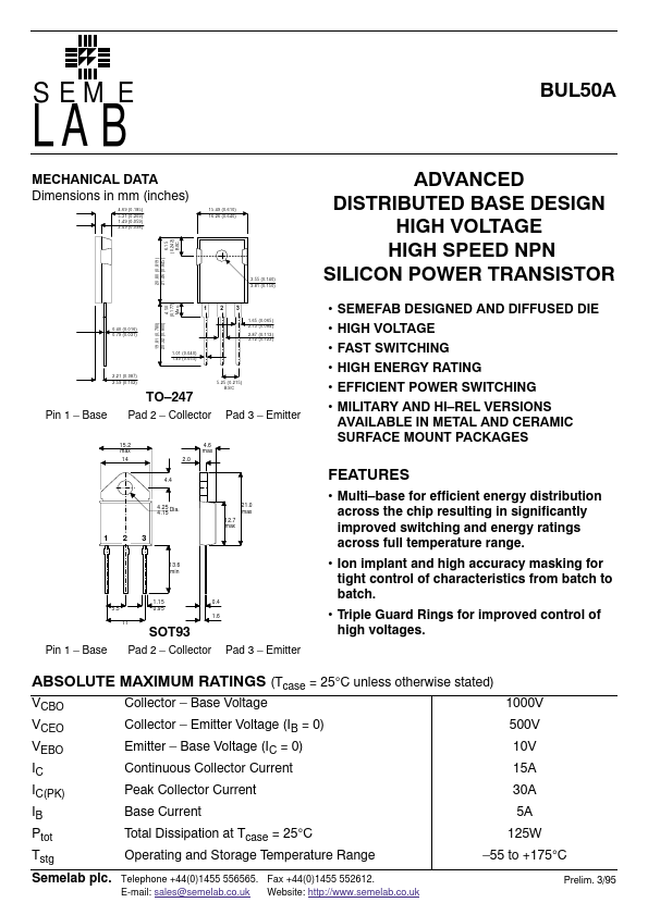
MECHANICAL DATA Dimensions in mm (inches)
4.69 5.31 1.49 2.49 (0.185) (0.209) (0.059) (0.098) 6.15 (0.242) BSC 15.49...
LAB
MECHANICAL DATA Dimensions in mm (inches)
4.69 5.31 1.49 2.49 (0.185) (0.209) (0.059) (0.098) 6.15 (0.242) BSC 15.49 (0.610) 16.26 (0.640) 20.80 (0.819) 21.46 (0.845) 3.55 (0.140) 3.81 (0.150)
SEME
BUL50A
ADVANCED DISTRIBUTED BASE DESIGN HIGH
VOLTAGE HIGH SPEED NPN SILICON POWER TRANSISTOR
SEMEFAB DESIGNED AND DIFFUSED DIE HIGH
VOLTAGE FAST SWITCHING HIGH ENERGY RATING EFFICIENT POWER SWITCHING MILITARY AND HI–REL VERSIONS AVAILABLE IN METAL AND CERAMIC SURFACE MOUNT PACKAGES
4.50 (0.177) M ax.
1
2
3
1.65 (0.065) 2.13 (0.084) 2.87 (0.113) 3.12 (0.123)
0.40 (0.016) 0.79 (0.031)
19.81 (0.780) 20.32 (0.800) 1.01 (0.040) 1.40 (0.055)
2.21 (0.087) 2.59 (0.102)
5.25 (0.215) BSC
TO–247
Pin 1 – Base Pad 2 – Collector
15.2 max 14 2.0 4.6 max
Pad 3 – Emitter
4.4
FEATURES
21.0 max 12.7 max
4.25 Dia. 4.15
1
2
3
Multi–base for efficient energy distribution across the chip resulting in significantly improved switching and energy ratings across full temperature range. Ion implant and high accuracy masking for tight control of characteristics from batch to batch. Triple Guard Rings for improved control of high
voltages.
13.6 min
5.5 11
1.15 0.95
0.4 1.6
SOT93
Pin 1 – Base Pad 2 – Collector Pad 3 – Emitter
ABSOLUTE MAXIMUM RATINGS (Tcase = 25°C unless otherwise stated)
VCBO VCEO VEBO IC IC(PK) IB Ptot Tstg Semelab plc. Collector – Base
Voltage Collector – Emitter
Voltage (IB = 0) Emitter – Base
Voltage (IC = 0) Continuous Collector Current Peak ...