isc N-Channel Mosfet Transistor
·FEATURES ·Static Drain-Source On-Resistance
: RDS(on) = 3.0Ω(Max) ·SOA is Power Dissip...
isc N-Channel
Mosfet Transistor
·FEATURES ·Static Drain-Source On-Resistance
: RDS(on) = 3.0Ω(Max) ·SOA is Power Dissipation Limited ·High speed switching ·Minimum Lot-to-Lot variations for robust device
performance and reliable operation
·DESCRITION Designed for applications such as switching regulators, switching converters, motor drivers,relay drivers and drivers for high power bipolar switching transistors requiring high speed and low gate
drive power.
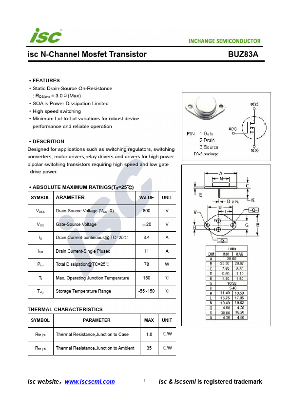
·ABSOLUTE MAXIMUM RATINGS(Ta=25℃)
SYMBOL ARAMETER
VALUE
UNIT
VDSS
Drain-Source
Voltage (VGS=0)
800
V
VGS
Gate-Source
Voltage
±20
V
ID
Drain Current-continuous@ TC=25℃
3.4
A
IDM
Drain Current-Single Plused
11
A
Ptot
Total Dissipation@TC=25℃
78
W
Tj
Max. Operating Junction Temperature
150
℃
Tstg
Storage Temperature Range
-55~150 ℃
THERMAL CHARACTERISTICS
SYMBOL
PARAMETER
MAX UNIT
Rth j-c Thermal Resistance,Junction to Case
1.6 ℃/W
Rth j-a Thermal Resistance,Junction to Ambient
35 ℃/W
BUZ83A
isc website:www.iscsemi.com
1 isc & iscsemi is registered trademark
isc N-Channel
Mosfet Transistor
ELECTRICAL CHARACTERISTICS
TC=25℃ unless otherwise specified
SYMBOL
PARAMETER
CONDITIONS
V(BR)DSS Drain-Source Breakdown
Voltage
VGS= 0; ID=0.25mA
VGS(th) Gate Threshold
Voltage
VDS= VGS; ID=1mA
VSD
Diode Forward On-
voltage
IS= 6.8A ;VGS= 0
RDS(on) Drain-Source On-Resistance
VGS= 10V; ID= 1.7A
IGSS
Gate-Body Leakage Current
VGS= ±20V;VDS= 0
IDSS
Zero Gate
Voltage Drain Current
V...