CAB450M12XM3
VDS
1200 V
5
4 IDS 3
450 A 2
1
1200 V, 2.6 mΩ, Silicon Carbide, Half-Bridge Module
D
Technical ...
CAB450M12XM3
VDS
1200 V
5
4 IDS 3
450 A 2
1
1200 V, 2.6 mΩ, Silicon Carbide, Half-Bridge Module
D
Technical Features
High Power Density Footprint High Junction Temperature (175 °C) Operation Low-Inductance (6.7 nH) Design Implements Conduction-Optimized Third
Generation SiC
MOSFET Technology
Silicon Nitride Insulator and Copper Baseplate
1200 V Drain-Source
Voltage
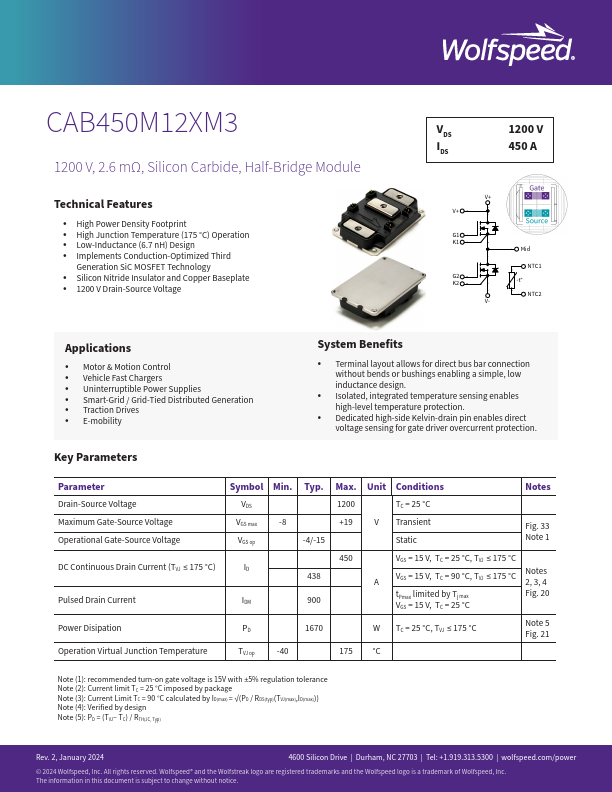
C
V+ V+
G1 K1
G2 K2
V-
Mid
NTC1 -t°
NTC2
Applications Motor & Motion Control Vehicle Fast Chargers Uninterruptible Power Supplies Smart-Grid / Grid-Tied Distributed Generation Traction Drives E-mobility
System Benefits
3 8,9
Terminal layout allows for direct bus bar connection
wBithout bends or bushings inductance design.
enab4ling
5
a
simple,
low
1
Isolated, integrated temperature sensing enables
high-level temperature protection.
10
Dedicated high-side Kelvin-drain67 pin enables dire-tc°t
voltage sensing for gate driver overcurrent protectio1n1 .
2
Key Parameters
A
Parameter
Symbol Min. Typ. Max. Unit Conditions
Notes
Drain-Source
Voltage Maximum Gate-Source
Voltage Operational Gate-Source
Voltage
VDS VGS max VGS op
1200
-8
+19
-4/-15
TC = 25 °C
5
4
V Transient
Static
3
2
1
Fig. 33
Note 1
DC Continuous Drain Current (TVJ ≤ 175 °C)
ID
Pulsed Drain Current
IDM
Power Disipation
PD
450 438 900
1670
VGS = 15 V, TC = 25 °C, TVJ ≤ 175 °C
A
VGS = 15 V, TC = 90 °C, TVJ ≤ 175 °C
Notes 2, 3, 4
tPmax limited by Tj max VGS = 15 V,...