Product Folder
Order Now
Technical Documents
Tools & Software
Support & Community
CD40106B
SCHS097F – NOVEMBER 1998...
Product Folder
Order Now
Technical Documents
Tools & Software
Support & Community
CD40106B
SCHS097F – NOVEMBER 1998 – REVISED MARCH 2017
CD40106B
CMOS Hex Schmitt-Trigger Inverters
1 Features
1 Schmitt-Trigger Inputs Hysteresis
Voltage (Typical):
– 0.9 V at VDD = 5 V – 2.3 V at VDD = 10 V – 3.5 V at VDD = 15 V Noise Immunity Greater Than 50% No Limit On Input Rise and Fall Times Standardized, Symmetrical Output Characteristics For Quiescent Current at 20 V Maximum Input Current Of 1 µA at 18 V Over Full Package Temperature Range: – 100 nA at 18 V and 25°C Low VDD and VSS Current During Slow Input Ramp 5-V, 10-V, and 15-V Parametric Ratings
2 Applications
Wave and Pulse Shapers High-Noise-Environment Systems Monostable Multivibrators Astable Multivibrators
3 Description
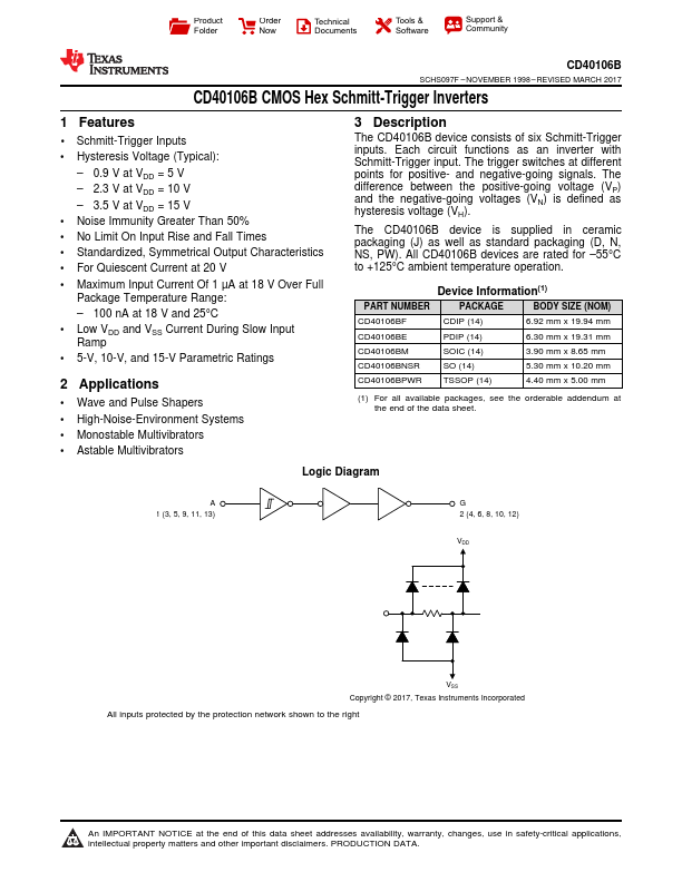
The CD40106B device consists of six Schmitt-Trigger inputs. Each circuit functions as an inverter with Schmitt-Trigger input. The trigger switches at different points for positive- and negative-going signals. The difference between the positive-going
voltage (VP) and the negative-going
voltages (VN) is defined as hysteresis
voltage (VH).
The CD40106B device is supplied in ceramic packaging (J) as well as standard packaging (D, N, NS, PW). All CD40106B devices are rated for –55°C to +125°C ambient temperature operation.
Device Information(1)
PART NUMBER
PACKAGE
BODY SIZE (NOM)
CD40106BF
CDIP (14)
6.92 mm x 19.94 mm
CD40106BE
PDIP (14)
6.30 mm x 19.31 mm
CD40106BM
SOIC ...