CD40109B-Q1
www.ti.com
SCHS380 A – JUNE 2010 – REVISED AUGUST 2011
CMOS QUAD LOW-TO-HIGH VOLTAGE SHIFTER
Check for Sam...
CD40109B-Q1
www.ti.com
SCHS380 A – JUNE 2010 – REVISED AUGUST 2011
CMOS QUAD LOW-TO-HIGH
VOLTAGE SHIFTER
Check for Samples: CD40109B-Q1
FEATURES
1
Qualified for Automotive Applications Independent of Power Supply Sequence
Considerations – VCC Can Exceed VDD – Input Signals can Exceed Both VCC and VDD Up and Down Level-Shifting Capability Three-State Outputs With Separate Enable Controls Standardized Symmetrical Output Characteristics 100% Tested for Quiescent Current at 20 V Maximum Input Current: – 1 µA at 18 V Over Full
Package-Temperature Range – 100 nA at 18 V and 25°C Noise Margin (Full Package-Temperature Range): – 1 V at VCC = 5 V, VDD = 10 V – 2 V at VCC = 10 V, VDD = 15 V 5-V, 10-V, and 15-V Parametric Ratings Meets All Requirements of JEDEC Tentative Standard No. 13B, "Standard specifications for
Description of 'B' Series
CMOS Devices" Latch-Up Performance Meets 50 mA per JESD
78, Class I
APPLICATIONS
High-or-Low Level-Shifting With Three-State Outputs for Unidirectional or Bidirectional Bussing
Isolation of Logic Subsystem Using Separate Power Supplies from Supply Sequencing, Supply Loss, and Supply Regulation Considerations
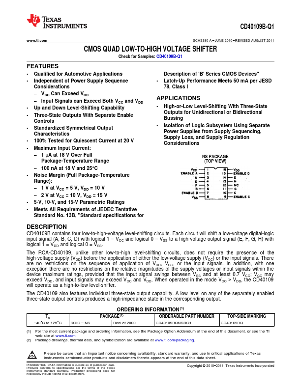
NS PACKAGE (TOP VIEW)
DESCRIPTION
CD40109B contains four low-to-high-
voltage level-shifting circuits. Each circuit will shift a low-
voltage digital-logic input signal (A, B, C, D) with logical 1 = VCC and logical 0 = VSS to a high-
voltage output signal (E, F, G, H) with logical 1 = VDD and logical 0 = VSS.
The RCA...