CD4010B-Q1
www.ti.com
SCHS379A – MARCH 2010 – REVISED JANUARY 2012
CMOS HEX BUFFER/CONVERTER
Check for Samples: CD4010...
CD4010B-Q1
www.ti.com
SCHS379A – MARCH 2010 – REVISED JANUARY 2012
CMOS HEX BUFFER/CONVERTER
Check for Samples: CD4010B-Q1
FEATURES
1
Qualified for Automotive Applications 100% Tested for Quiescent Current at 20 V Maximum Input Current of 1 µA at 18 V Over
Full Package-Temperature Range: 100 nA at 18 V and 25°C 5-V, 10-V, and 15-V Parametric Ratings Latch-Up Performance Meets 100 mA per JESD 78, Class I
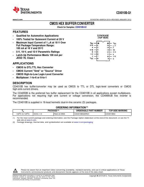
D PACKAGE (TOP VIEW)
APPLICATIONS
CMOS to DTL/TTL Hex Converter
CMOS Current "Sink" or "Source" Driver
CMOS High-to-Low Logic-Level Converter Multiplexer: 1-to-6 or 6-to-1
DESCRIPTION
CD4010B hex buffer/converter may be used as
CMOS to TTL or DTL logic-level converters or
CMOS high-sink-current drivers.
The CD4050B is the preferred hex buffer replacement for the CD4010B in all applications except multiplexers. For applications not requiring high sink current or
voltage conversion, the CD4069UB hex inverter is recommended.
The CD4010B is supplied in 16-lead hermetic dual-in-line ceramic (D) packages.
TA –40°C to 125°C
SOIC – D
ORDERING INFORMATION(1)
PACKAGE (2)
ORDERABLE PART NUMBER
Reel of 2500
CD4010BQDRQ1
TOP-SIDE MARKING CD4010BQ
(1) For the most current package and ordering information, see the Package Option Addendum at the end of this document, or see the TI web site at www.ti.com.
(2) Package drawings, thermal data, and symbolization are available at www.ti.com/packaging.
1
Please be aware that an important notice concerning availabili...