CD4021B-Q1
www.ti.com
CMOS 8-STAGE STATIC SHIFT REGISTER
Check for Samples: CD4021B-Q1
SCHS378 – MARCH 2010
FEATURES...
CD4021B-Q1
www.ti.com
CMOS 8-STAGE STATIC SHIFT REGISTER
Check for Samples: CD4021B-Q1
SCHS378 – MARCH 2010
FEATURES
1
Qualified for Automotive Applications Medium-Speed Operation: 12-MHz (Typ) Clock
Rate at VDD – VSS = 10 V Fully Static Operation Eight Master-Slave Flip-Flops Plus Output
Buffering and Control Gating 100% Tested for Quiescent Current at 20 V Maximum Input Current of 1 µA at 18 V Over
Full Package-Temperature Range: 100 nA at 18 V and 25°C Noise Margin (Full Package-Temperature Range): – 1 V at VDD = 5 V – 2 V at VDD = 10 V – 2.5 V at VDD = 15 V Standardized Symmetrical Output Characteristics 5-V, 10-V, and 15-V Parametric Ratings
Meets All Requirements of JEDEC Tentative Standard No. 13B, "Standard Specifications for Description of 'B' Series
CMOS Devices"
Latch-Up Performance Meets 50 mA per JESD 78, Class I
APPLICATIONS
Parallel Input/Serial Output Data Queuing Parallel-to-Serial Data Conversion General-Purpose Register
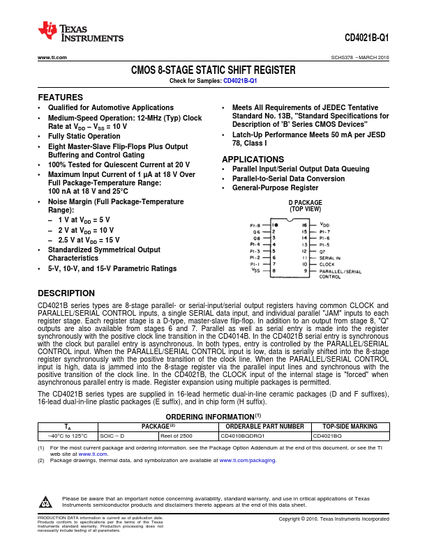
D PACKAGE (TOP VIEW)
DESCRIPTION
CD4021B series types are 8-stage parallel- or serial-input/serial output registers having common CLOCK and PARALLEL/SERIAL CONTROL inputs, a single SERIAL data input, and individual parallel "JAM" inputs to each register stage. Each register stage is a D-type, master-slave flip-flop. In addition to an output from stage 8, "Q" outputs are also available from stages 6 and 7. Parallel as well as serial entry is made into the register synchronously with the positive clock line tr...