CD54HC166, CD54HCT166, CD74HC166, CD74HCT166
SCHS157D – FEBRUARY 1998 – REVISED FEBRUARY 2022
CDx4HC(T)166 High-Speed CM...
CD54HC166, CD54HCT166, CD74HC166, CD74HCT166
SCHS157D – FEBRUARY 1998 – REVISED FEBRUARY 2022
CDx4HC(T)166 High-Speed
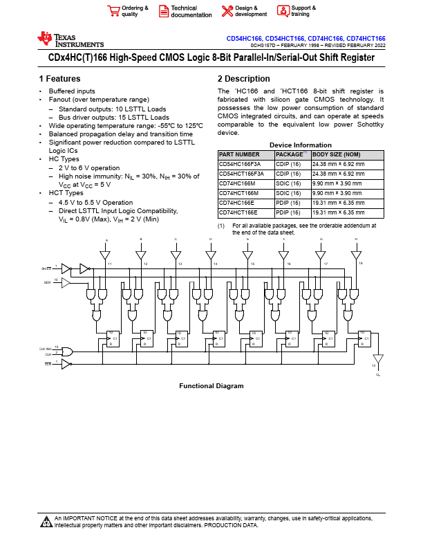
CMOS Logic 8-Bit Parallel-In/Serial-Out Shift Register
1 Features
2 Description
Buffered inputs
The ’HC166 and ’HCT166 8-bit shift register is
Fanout (over temperature range)
fabricated with silicon gate
CMOS technology. It
– Standard outputs: 10 LSTTL Loads
– Bus driver outputs: 15 LSTTL Loads
Wide operating temperature range: -55℃ to 125℃ Balanced propagation delay and transition time
possesses the low power consumption of standard
CMOS integrated circuits, and can operate at speeds comparable to the equivalent low power Schottky device.
Significant power reduction compared to LSTTL Logic ICs
HC Types
– 2 V to 6 V operation – High noise immunity: NIL = 30%, NIH = 30% of
VCC at VCC = 5 V HCT Types
PART NUMBER
Device Information
PACKAGE(1) BODY SIZE (NOM)
CD54HC166F3A
CDIP (16) 24.38 mm × 6.92 mm
CD54HCT166F3A CDIP (16) 24.38 mm × 6.92 mm
CD74HC166M
SOIC (16) 9.90 mm × 3.90 mm
CD74HCT166M
SOIC (16) 9.90 mm × 3.90 mm
– 4.5 V to 5.5 V Operation
CD74HC166E
PDIP (16) 19.31 mm × 6.35 mm
– Direct LSTTL Input Logic Compatibility, VIL = 0.8V (Max), VIH = 2 V (Min)
CD74HCT166E
PDIP (16) 19.31 mm × 6.35 mm
(1) For all available packages, see the orderable addendum at the end of the data sheet.
A
B
C
D
E
F
G
H
1 SH/LD
10 SER
11
12
13
14
15
16
17
18
15 CLK INH
2 CLK
1 CLR
1D C1
R
1D C1
R
1D C1
R
1D C1
R
1D C1
R...