Data sheet acquired from Harris Semiconductor SCHS280C
November 1997 - Revised July 2003
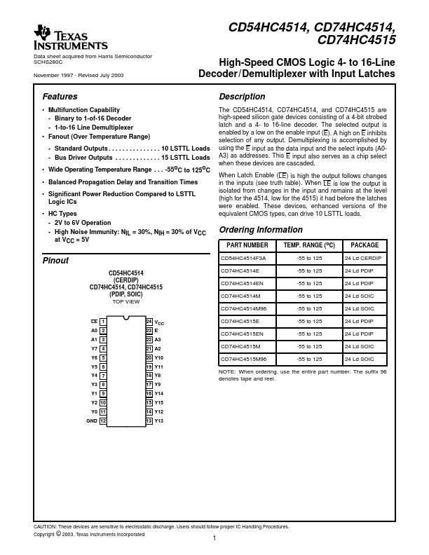
CD54HC4514, CD74HC4514, CD74HC...
Data sheet acquired from Harris Semiconductor SCHS280C
November 1997 - Revised July 2003
CD54HC4514, CD74HC4514, CD74HC4515
High-Speed
CMOS Logic 4- to 16-Line Decoder/Demultiplexer with Input Latches
[ /Title (CD74 HC451 4, CD74 HC451 5) /Subject (High Speed
CMOS
Features
Description
Multifunction Capability - Binary to 1-of-16 Decoder - 1-to-16 Line Demultiplexer
Fanout (Over Temperature Range)
- Standard Outputs . . . . . . . . . . . . . . . 10 LSTTL Loads - Bus Driver Outputs . . . . . . . . . . . . . 15 LSTTL Loads Wide Operating Temperature Range . . . -55oC to 125oC
Balanced Propagation Delay and Transition Times
Significant Power Reduction Compared to LSTTL Logic ICs
HC Types - 2V to 6V Operation - High Noise Immunity: NIL = 30%, NIH = 30% of VCC at VCC = 5V
The CD54HC4514, CD74HC4514, and CD74HC4515 are high-speed silicon gate devices consisting of a 4-bit strobed latch and a 4- to 16-line decoder. The selected output is enabled by a low on the enable input (E). A high on E inhibits selection of any output. Demultiplexing is accomplished by using the E input as the data input and the select inputs (A0A3) as addresses. This E input also serves as a chip select when these devices are cascaded.
When Latch Enable (LE) is high the output follows changes in the inputs (see truth table). When LE is low the output is isolated from changes in the input and remains at the level (high for the 4514, low for the 4515) it had before the latches were enabled. These...