CD54HC374, CD74HC374, CD54HCT374, CD74HCT374, CD54HC574, CD74HC574, CD54HCT574, CD74HCT574
SCHS183E – NOVEMBER 1998 – RE...
CD54HC374, CD74HC374, CD54HCT374, CD74HCT374, CD54HC574, CD74HC574, CD54HCT574, CD74HCT574
SCHS183E – NOVEMBER 1998 – REVISED OCTOBER 2022
CDx4HC374 High-Speed
CMOS Logic Octal D-Type Flip-Flop, 3-State Positive-Edge Triggered
1 Features
Buffered inputs Common three-state output enable control Three-state outputs Bus line driving capability Typical propagation delay (clock to Q) = 15 ns at
VCC = 5 V, CL = 15 pF, TA = 25℃ Fanout (over temperature range)
– Standard outputs: 10 LSTTL loads – Bus driver outputs: 15 LSTTL loads Wide operating temperature range: –55℃ to 125℃ Balanced propagation delay and transition times Significant power reduction compared to LSTTL Logic ICs HC types
– 2-V to 6-V operation – High noise immunity: NIL = 30%, NIH = 30% of
VCC at VCC = 5 V HCT types
– 4.5-V to 5.5-V Operation – Direct LSTTL input logic compatibility,
VIL = 0.8 V (max), VIH = 2 V (min) –
CMOS input compatibility, II ≤ 1μA at VOL, VOH
2 Description
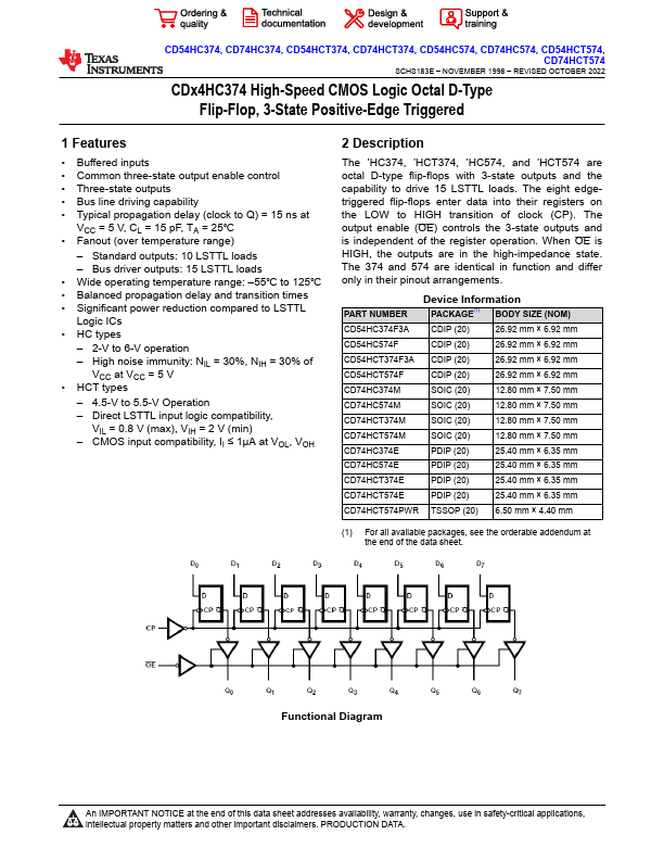
The ’HC374, ’HCT374, ’HC574, and ’HCT574 are octal D-type flip-flops with 3-state outputs and the capability to drive 15 LSTTL loads. The eight edgetriggered flip-flops enter data into their registers on the LOW to HIGH transition of clock (CP). The output enable (OE) controls the 3-state outputs and is independent of the register operation. When OE is HIGH, the outputs are in the high-impedance state. The 374 and 574 are identical in function and differ only in their pinout arrangements.
PART NUMBER
Device Informa...