CD54HC4511, CD74HC4511, CD74HCT4511
SCHS279E – DECEMBER 1998 – REVISED AUGUST 2022
CDx4HC4511, CD74HCT4511 BCD-to-7 Segm...
CD54HC4511, CD74HC4511, CD74HCT4511
SCHS279E – DECEMBER 1998 – REVISED AUGUST 2022
CDx4HC4511, CD74HCT4511 BCD-to-7 Segment Latch/Decoder/Drivers
1 Features
2-V to 6-V VCC operation ('HC4511) 4.5-V to 5.5-V VCC operation (CD74HCT4511) High-output sourcing capability
– 7.5 mA at 4.5 V (CD74HCT4511) – 10 mA at 6 V ('HC4511) Input latches for BCD code storage Lamp test and blanking capability Balanced propagation delays and transition times Significant power reduction compared to LSTTL logic IC's 'HC4511
– High noise immunity, NIL or NIH = 30% of VCC at VCC = 5 V
CD74HCT4511
– Direct LSTTL input logic compatibility, VIL = 0.8 V Maximum, VIH = 2 V minimum
–
CMOS input compatibility, II ≤ 1μA at VOL, VOH
2 Description
The
CD54HC4511,
CD74HC4511,
and
CD74HCT4511 are BCD-to-7 segment latch/decoder/
drivers with four address inputs (D0−D3), an activelow blanking (BL) input, lamp-test (LT) input, and a
latch-enable (LE) input that, when high, enables the
latches to store the BCD inputs. When LE is low, the
latches are disabled, making the outputs transparent
to the BCD inputs.
PART NUMBER CD54HC4511 CD74HC4511
CD74HCT4511
Device Information
PACKAGE(1)
BODY SIZE (NOM)
J (CDIP, 16)
24.38 mm × 6.92 mm
N (PDIP, 16)
19.31 mm × 6.35 mm
D (SOIC, 16)
9.90 mm × 3.90 mm
PW (TSSOP, 16) 5.00 mm × 4.40 mm
N (PDIP, 16)
19.31 mm × 6.35 mm
(1) For all available packages, see the orderable addendum at the end of the data sheet.
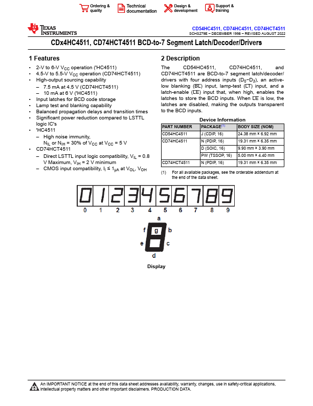
Display
An IMPORTANT NOTICE ...