SMD Schottky Barrier Diode
SMD Diodes Specialist
CDBU0230-N (Lead-free Device)
Io = 200 mA V R = 30 Volt s Features
Des...
SMD Schottky Barrier Diode
SMD Diodes Specialist
CDBU0230-N (Lead-free Device)
Io = 200 mA V R = 30 Volt s Features
Designed for mounting on small surface. Extremely thin/leadless package. Low drop-down
voltage. Majority carrier conduction.
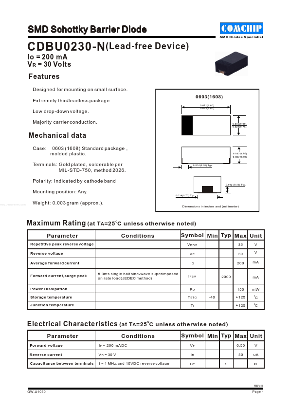
0.035(0.90) 0.029(0.75)
0603(1608)
0.071(1.80) 0.063(1.60)
Mechanical data
Case: 0603 (1608) Standard package , molded plastic.
0.014(0.35) Typ. 0.033(0.85) 0.027(0.70)
Terminals: Gold plated, solderable per MIL-STD-750, method 2026. Polarity: Indicated by cathode band
0.012 (0.30) Typ.
Mounting position: Any.
0.028(0.70) Typ.
www.DataSheet4U.com
Weight: 0.003 gram (approx.).
Dimensions in inches and (millimeter)
Maximum Rating (at TA =25 C unless otherwise noted)
O
Parameter
Repetitive peak reverse
voltage Reverse
voltage Average forward current Forward current,surge peak Power Dissipation Storage temperature Junction temperature
Conditions
Symbol Min Typ Max Unit
V RRM VR IO 35 30 200 V V mA
8.3ms single half sine-wave superimposed on rate load(JEDEC method)
I FSM PD T STG Tj -40
2000 150 +125 +125
mA mW
O
C C
O
Electrical Characteristics (at TA =25 C unless otherwise noted)
O
Parameter
Forward
voltage Reverse current Capacitance between terminals V R = 30 V
Conditions
I F = 200 mA DC
Symbol Min Typ Max Unit
VF IR CT 9 0.50 30 V uA
PF
f = 1 MH Z ,and 10VDC reverse
voltage
REV:B
QW-A1050
Page 1
SMD Schottky Barrier Diode
SMD Diodes Specialist
RATING AND CHARACTERISTIC CURVES (CDBU0230-N)
Fig. 1 - Forward chara...