CDC111 1-LINE TO 9-LINE DIFFERENTIAL LVPECL CLOCK DRIVER
D Low-Output Skew for Clock-Distribution
Applications
D Differ...
CDC111 1-LINE TO 9-LINE DIFFERENTIAL LVPECL CLOCK DRIVER
D Low-Output Skew for Clock-Distribution
Applications
D Differential Low-
Voltage Pseudo-ECL
(LVPECL)-Compatible Inputs and Outputs
D Distributes Differential Clock Inputs to Nine
Differential Clock Outputs
D Output Reference
Voltage, VREF , Allows
Distribution From a Single-Ended Clock Input
D Single-Ended LVPECL-Compatible Output
Enable
D Packaged in Plastic Chip Carrier
description
SCAS321G – SEPTEMBER 1993 – REVISED AUGUST 1999
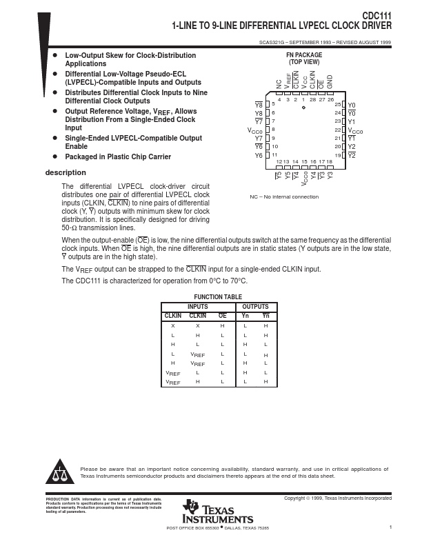
FN PACKAGE (TOP VIEW)
NC VREF CLKIN V CC CLKIN OE GND
Y8 Y8 Y7 VCC0 Y7 Y6 Y6
4 3 2 1 28 27 26 5 25 6 24 7 23 8 22 9 21 10 20 11 19
12 13 14 15 16 17 18
Y0 Y0 Y1 VCC0 Y1 Y2 Y2
Y5 Y5 Y4 VCC0 Y4 Y3 Y3
The differential LVPECL clock-driver circuit distributes one pair of differential LVPECL clock inputs (CLKIN, CLKIN) to nine pairs of differential clock (Y, Y) outputs with minimum skew for clock distribution. It is specifically designed for driving 50-Ω transmission lines.
NC – No internal connection
When the output-enable (OE) is low, the nine differential outputs switch at the same frequency as the differential clock inputs. When OE is high, the nine differential outputs are in static states (Y outputs are in the low state, Y outputs are in the high state).
The VREF output can be strapped to the CLKIN input for a single-ended CLKIN input. The CDC111 is characterized for operation from 0°C to 70°C.
FUNCTION TABLE
INPUTS
OUTPUTS
CLKIN CLKIN OE
Yn Yn
X X H LH
L H L LH
H L L HL
L ...