CDC340 1-LINE TO 8-LINE CLOCK DRIVER
D Low Output Skew, Low Pulse Skew for
Clock-Distribution and Clock-Generation
Appl...
CDC340 1-LINE TO 8-LINE CLOCK DRIVER
D Low Output Skew, Low Pulse Skew for
Clock-Distribution and Clock-Generation
Applications
D TTL-Compatible Inputs and Outputs D Distributes One Clock Input to Eight
Outputs
D Distributed VCC and Ground Pins Reduce
Switching Noise
D High-Drive Outputs (– 48-mA IOH,
48-mA IOL)
D State-of-the-Art EPIC-ΙΙB™ Bi
CMOS Design
Significantly Reduces Power Dissipation
D Package Options Include Plastic
Small-Outline (DW) and Shrink
SCAS332B – DECEMBER 1992 – REVISED MAY 1997
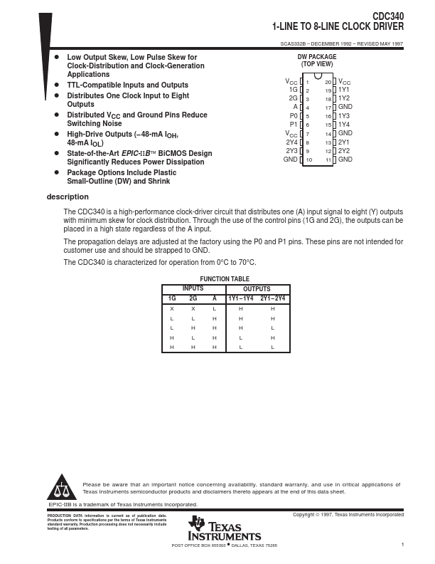
DW PACKAGE (TOP VIEW)
VCC 1 1G 2 2G 3 A4 P0 5 P1 6
VCC 7 2Y4 8 2Y3 9 GND 10
20 VCC 19 1Y1 18 1Y2 17 GND 16 1Y3 15 1Y4 14 GND 13 2Y1 12 2Y2 11 GND
description
The CDC340 is a high-performance clock-driver circuit that distributes one (A) input signal to eight (Y) outputs with minimum skew for clock distribution. Through the use of the control pins (1G and 2G), the outputs can be placed in a high state regardless of the A input.
The propagation delays are adjusted at the factory using the P0 and P1 pins. These pins are not intended for customer use and should be strapped to GND.
The CDC340 is characterized for operation from 0°C to 70°C.
FUNCTION TABLE
INPUTS
OUTPUTS
1G 2G
A 1Y1 – 1Y4 2Y1 – 2Y4
X
X
L
H
H
L
L
H
H
H
L
H
H
H
L
H
L
H
L
H
H
H
H
L
L
Please be aware that an important notice concerning availability, standard warranty, and use in critical applications of Texas Instruments semiconductor products and disclaimers thereto appears at the end of...