Product Folder
Sample & Buy
Technical Documents
Tools & Software
Support & Community
Reference Design
CDCE913-Q1, ...
Product Folder
Sample & Buy
Technical Documents
Tools & Software
Support & Community
Reference Design
CDCE913-Q1, CDCEL913-Q1
SCAS918C – JUNE 2013 – REVISED NOVEMBER 2016
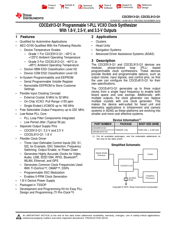
CDCEx913-Q1 Programmable 1-PLL VCXO Clock Synthesizer With 1.8-V, 2.5-V, and 3.3-V Outputs
1 Features
1 Qualified for Automotive Applications AEC-Q100 Qualified With the Following Results:
– Device Temperature Grades – Grade 1 For CDCE913-Q1: –40°C to +125°C Ambient Operating Temperature – Grade 3 For CDCEL913-Q1: –40°C to +85°C Ambient Operating Temperature
– Device HBM ESD Classification Level H2 – Device CDM ESD Classification Level C6 In-System Programmability and EEPROM – Serial Programmable Volatile Register – Nonvolatile EEPROM to Store Customer
Settings Flexible Input Clocking Concept
– External Crystal: 8 MHz to 32 MHz – On-Chip VCXO: Pull Range ±150 ppm – Single-Ended LV
CMOS up to 160 MHz Free Selectable Output Frequency up to 230 MHz Low-Noise PLL Core – PLL Loop Filter Components Integrated – Low Period Jitter (Typical 50 ps) Separate Output Supply Pins – CDCE913-Q1: 3.3 V and 2.5 V – CDCEL913-Q1: 1.8 V Flexible Clock Driver – Three User-Definable Control Inputs [S0, S1,
S2], for Example, SSC Selection, Frequency Switching, Output Enable, or Power Down – Generates Highly Accurate Clocks for Video, Audio, USB, IEEE1394, RFID, Bluetooth®, WLAN, Ethernet, and GPS – Generates Common Clock Frequencies Used With TI-DaVinci™, OMAP™, DSPs – Programmable SSC Modulation – Enables 0-PP...