CDCE949-Q1
www.ti.com
SCAS891 – FEBRUARY 2010
PROGRAMMABLE 4-PLL VCXO CLOCK SYNTHESIZER WITH 1.8-V, 2.5-,V and 3.3-V L...
CDCE949-Q1
www.ti.com
SCAS891 – FEBRUARY 2010
PROGRAMMABLE 4-PLL VCXO CLOCK SYNTHESIZER WITH 1.8-V, 2.5-,V and 3.3-V LV
CMOS OUTPUTS
Check for Samples: CDCE949-Q1
FEATURES
1
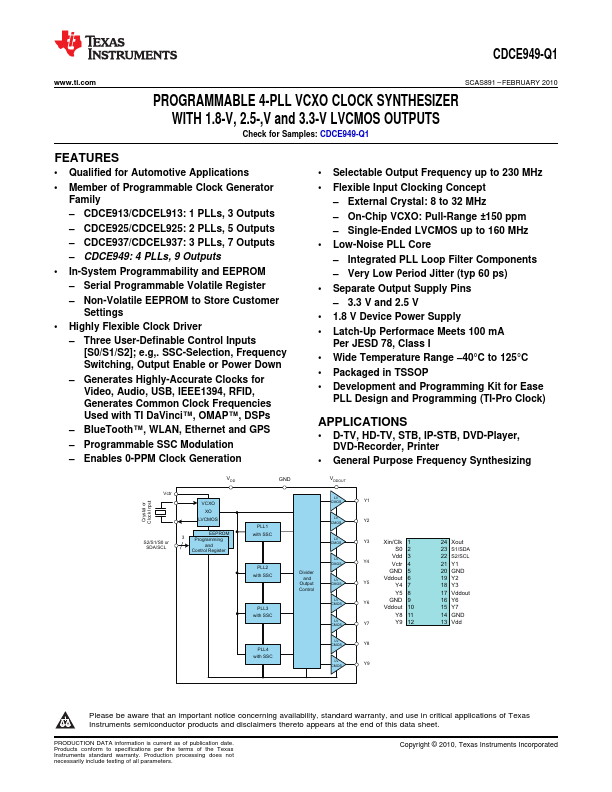
Qualified for Automotive Applications Member of Programmable Clock Generator
Family – CDCE913/CDCEL913: 1 PLLs, 3 Outputs – CDCE925/CDCEL925: 2 PLLs, 5 Outputs – CDCE937/CDCEL937: 3 PLLs, 7 Outputs – CDCE949: 4 PLLs, 9 Outputs In-System Programmability and EEPROM – Serial Programmable Volatile Register – Non-Volatile EEPROM to Store Customer
Settings Highly Flexible Clock Driver
– Three User-Definable Control Inputs [S0/S1/S2]; e.g,. SSC-Selection, Frequency Switching, Output Enable or Power Down
– Generates Highly-Accurate Clocks for Video, Audio, USB, IEEE1394, RFID, Generates Common Clock Frequencies Used with TI DaVinci™, OMAP™, DSPs
– BlueTooth™, WLAN, Ethernet and GPS – Programmable SSC Modulation – Enables 0-PPM Clock Generation
Selectable Output Frequency up to 230 MHz Flexible Input Clocking Concept
– External Crystal: 8 to 32 MHz – On-Chip VCXO: Pull-Range ±150 ppm – Single-Ended LV
CMOS up to 160 MHz Low-Noise PLL Core – Integrated PLL Loop Filter Components – Very Low Period Jitter (typ 60 ps) Separate Output Supply Pins – 3.3 V and 2.5 V 1.8 V Device Power Supply Latch-Up Performace Meets 100 mA Per JESD 78, Class I Wide Temperature Range –40°C to 125°C Packaged in TSSOP Development and Programming Kit for Ease PLL Design and Programming (TI-Pro Clock)
APPLICATIONS...