3.3-V Phase-Lock Loop Clock Driver
CDCF2510 3.3ĆV PHASEĆLOCK LOOP CLOCK DRIVER
ą
SCAS628D − APRIL 1999 − REVISED DECEMBER 2004
D Use CDCVF2510A as a Repla...
Description
CDCF2510 3.3ĆV PHASEĆLOCK LOOP CLOCK DRIVER
ą
SCAS628D − APRIL 1999 − REVISED DECEMBER 2004
D Use CDCVF2510A as a Replacement for
this Device
D Designed to Meet PC133 SDRAM
Registered DIMM Specification Rev. 0.9
D Spread Spectrum Clock Compatible D Operating Frequency 25 MHz to 140 MHz D Static Phase Error Distribution at 66 MHz
to 133 MHz is ±125 ps
D Jitter (cyc−cyc) at 66 MHz to 133 MHz Is
|70| ps
D Available in Plastic 24-Pin TSSOP D Phase-Lock Loop Clock Distribution for
Synchronous DRAM Applications
D Distributes One Clock Input to One Bank of
10 Outputs
D Output Enable Pin to Enable/Disable All 10
Outputs
D External Feedback (FBIN) Terminal Is Used
to Synchronize the Outputs to the Clock Input
D On-Chip Series Damping Resistors D No External RC Network Required D Operates at 3.3 V
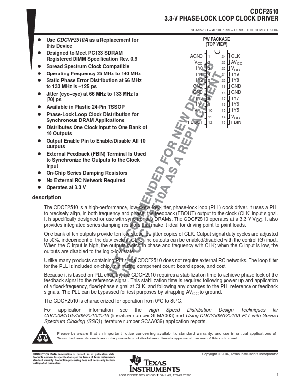
PW PACKAGE (TOP VIEW)
AGND 1 VCC 2 1Y0 3 1Y1 4 1Y2 5 GND 6 GND 7 1Y3 8 1Y4 9 VCC 10 G 11
FBOUT 12
24 CLK 23 AVCC 22 VCC 21 1Y9 20 1Y8 19 GND 18 GND 17 1Y7 16 1Y6 15 1Y5 14 VCC 13 FBIN
description
The CDCF2510 is a high-performance, low-skew, low-jitter, phase-lock loop (PLL) clock driver. It uses a PLL to precisely align, in both frequency and phase, the feedback (FBOUT) output to the clock (CLK) input signal. It is specifically designed for use with synchronous DRAMs. The CDCF2510 operates at a 3.3-V VCC. It also provides integrated series-damping resistors that make it ideal for driving point-to-point loads.
One bank of ten outputs provide ten low-skew, low-jitter copies of CLK. Outpu...
Similar Datasheet