Product Folder
Order Now
Technical Documents
Tools & Software
Support & Community
CDCLVC1102, CDCLVC1103, CDCLVC110...
Product Folder
Order Now
Technical Documents
Tools & Software
Support & Community
CDCLVC1102, CDCLVC1103, CDCLVC1104 CDCLVC1106, CDCLVC1108, CDCLVC1110, CDCLVC1112
SCAS895B – MAY 2010 – REVISED FEBRUARY 2017
CDCLVC11xx 3.3-V and 2.5-V LV
CMOS High-Performance Clock Buffer Family
1 Features
1 High-Performance 1:2, 1:3, 1:4, 1:6, 1:8, 1:10, 1:12 LV
CMOS Clock Buffer Family
Very Low Pin-to-Pin Skew < 50 ps Very Low Additive Jitter < 100 fs Supply
Voltage: 3.3 V or 2.5 V fmax = 250 MHz for 3.3 V
fmax = 180 MHz for 2.5 V Operating Temperature Range: –40°C to 85°C Available in 8-, 14-, 16-, 20-, 24-Pin TSSOP
Package (All Pin-Compatible)
2 Applications
General-Purpose Communication, Industrial, and Consumer Applications
3 Description
The CDCLVC11xx is a modular, high-performance, low-skew, general-purpose clock buffer family from Texas Instruments.
The entire family is designed with a modular approach in mind. It is intended to round up TI's series of LV
CMOS clock generators.
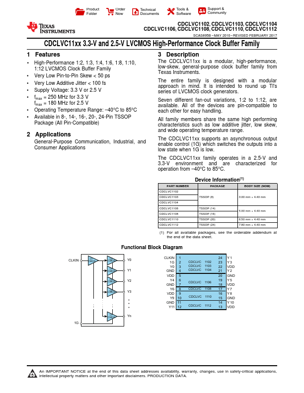
Seven different fan-out variations, 1:2 to 1:12, are available. All of the devices are pin-compatible to each other for easy handling.
All family members share the same high performing characteristics such as low additive jitter, low skew, and wide operating temperature range.
The CDCLVC11xx supports an asynchronous output enable control (1G) which switches the outputs into a low state when 1G is low.
The CDCLVC11xx family operates in a 2.5-V and 3.3-V environment and are characterized for ope...