CDCLVD2104
www.ti.com
SCAS903A – JUNE 2010 – REVISED AUGUST 2010
Dual 1:4 Low Additive Jitter LVDS Buffer
Check for Sa...
CDCLVD2104
www.ti.com
SCAS903A – JUNE 2010 – REVISED AUGUST 2010
Dual 1:4 Low Additive Jitter LVDS Buffer
Check for Samples: CDCLVD2104
FEATURES
1
Dual 1:4 Differential Buffer Low Additive Jitter <300 fs, RMS in
10 kHz to 20 MHz Low Within Bank Output Skew of 35ps (Max) Universal Inputs Accept LVDS, LVPECL,
LV
CMOS One Input Dedicated for Four Output Buffers 8 LVDS Outputs, ANSI EIA/TIA-644A Standard
Compatible Clock Frequency up to 800 MHz 2.375–2.625V Device Power Supply LVDS Reference
Voltage, VAC_REF, Available for
Capacitive Coupled Inputs Industrial Temperature Range –40°C to 85°C Packaged in 5mm × 5mm 28-Pin QFN (RHD) ESD Protection Exceeds 3 kV HBM, 1 kV CDM
APPLICATIONS
Telecommunications/Networking Medical Imaging Test and Measurement Equipment Wireless Communications General Purpose Clocking
DESCRIPTION
The CDCLVD2104 clock buffer distributes two clock inputs (IN0, IN1) to a total of 8 pairs of differential LVDS clock outputs (OUT0, OUT7). Each buffer block consists of one input and 4 LVDS outputs. The inputs can either be LVDS, LVPECL, or LV
CMOS.
The CDCLVD2104 is specifically designed for driving 50-Ω transmission lines. If the input is in single ended mode, the appropriate bias
voltage (VAC_REF) should be applied to the unused negative input pin.
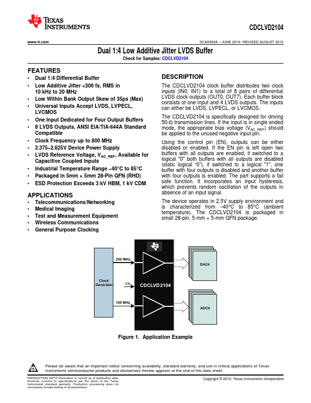
Using the control pin (EN), outputs can be either disabled or enabled. If the EN pin is left open two buffers with all outputs are enabled, if switched to a logical "0" both buffers ...