Product Folder
Sample & Buy
Technical Documents
Tools & Software
Support & Community
CDCLVP1102
SCAS884D – AUGUST 2...
Product Folder
Sample & Buy
Technical Documents
Tools & Software
Support & Community
CDCLVP1102
SCAS884D – AUGUST 2009 – REVISED DECEMBER 2015
CDCLVP1102 Two-LVPECL Output, High-Performance Clock Buffer
1 Features
1 1:2 Differential Buffer Single Clock Input Universal Inputs Can Accept LVPECL, LVDS,
LV
CMOS/LVTTL Two LVPECL Outputs Maximum Clock Frequency: 2 GHz Maximum Core Current Consumption: 33 mA Very Low Additive Jitter: <100 fs, RMS in 10-kHz
to 20-MHz Offset Range 2.375-V to 3.6-V Device Power Supply Maximum Propagation Delay: 450 ps Maximum Output Skew: 10 ps LVPECL Reference
Voltage, VAC_REF, Available
for Capacitive-Coupled Inputs Industrial Temperature Range: –40°C to 85°C Supports 105°C PCB Temperature (Measured at
Thermal Pad) Available in 3-mm × 3-mm QFN-16 (RGT)
Package ESD Protection Exceeds 2 kV (HBM)
2 Applications
Wireless Communications Telecommunications/Networking Medical Imaging Test and Measurement Equipment
3 Description
The CDCLVP1102 is a highly versatile, low additive jitter buffer that can generate two copies of LVPECL clock outputs from one LVPECL, LVDS, or LV
CMOS input for a variety of communication applications. It has a maximum clock frequency up to 2 GHz. The overall additive jitter performance is less than 0.1 ps, RMS from 10 kHz to 20 MHz, and overall output skew is as low as 10 ps, making the device a perfect choice for use in demanding applications.
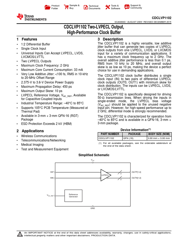
The CDCLVP1102 clock buffer distributes a sing...