Product Folder
Sample & Buy
Technical Documents
Tools & Software
Support & Community
Reference Design
CDCLVP1204
S...
Product Folder
Sample & Buy
Technical Documents
Tools & Software
Support & Community
Reference Design
CDCLVP1204
SCAS880F – AUGUST 2009 – REVISED SEPTEMBER 2015
CDCLVP1204 Four LVPECL Output, High-Performance Clock Buffer
1 Features
1 2:4 Differential Buffer Selectable Clock Inputs Through Control Terminal Universal Inputs Accept LVPECL, LVDS, and
LV
CMOS/LVTTL Four LVPECL Outputs Maximum Clock Frequency: 2 GHz Maximum Core Current Consumption: 45 mA Very Low Additive Jitter: <100 fs, RMS in 10-kHz
to 20-MHz Offset Range: – 57 fs, RMS (typical) at 122.88 MHz – 48 fs, RMS (typical) at 156.25 MHz – 30 fs, RMS (typical) at 312.5 MHz 2.375-V to 3.6-V Device Power Supply Maximum Propagation Delay: 450 ps Maximum Output Skew: 15 ps LVPECL Reference
Voltage, VAC_REF, Available for Capacitive-Coupled Inputs Industrial Temperature Range: –40°C to +85°C Supports 105°C PCB Temperature (Measured at Thermal Pad) ESD Protection Exceeds 2 kV (HBM)
2 Applications
Wireless Communications Telecommunications/Networking Medical Imaging Test and Measurement Equipment
3 Description
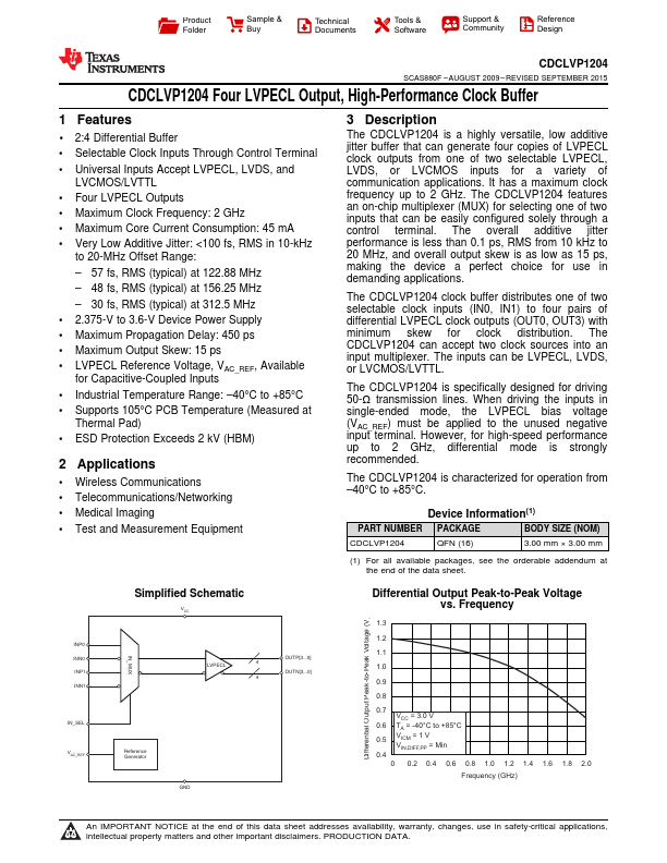
The CDCLVP1204 is a highly versatile, low additive jitter buffer that can generate four copies of LVPECL clock outputs from one of two selectable LVPECL, LVDS, or LV
CMOS inputs for a variety of communication applications. It has a maximum clock frequency up to 2 GHz. The CDCLVP1204 features an on-chip multiplexer (MUX) for selecting one of two inputs that can be easily configure...