Product Folder
Sample & Buy
Technical Documents
Tools & Software
Support & Community
CDCLVP2108
SCAS878C – MAY 2009...
Product Folder
Sample & Buy
Technical Documents
Tools & Software
Support & Community
CDCLVP2108
SCAS878C – MAY 2009 – REVISED JANUARY 2016
CDCLVP2108 16-LVPECL Output, High-Performance Clock Buffer
1 Features
1 Dual 1:8 Differential Buffer Two Clock Inputs Universal Inputs Can Accept LVPECL, LVDS,
LV
CMOS/LVTTL 16 LVPECL Outputs Maximum Clock Frequency: 2 GHz Maximum Core Current Consumption: 115 mA Very Low Additive Jitter: <100 fs, RMS in 10-kHz
to 20-MHz Offset Range 2.375-V to 3.6-V Device Power Supply Maximum Propagation Delay: 550 ps Maximum Within Bank Output Skew: 25 ps LVPECL Reference
Voltage, VAC_REF, Available
for Capacitive-Coupled Inputs Industrial Temperature Range: –40°C to +85°C Supports 105°C PCB Temperature (Measured
with a Thermal Pad) Available in 7-mm × 7-mm, 48-Pin VQFN (RGZ)
Package ESD Protection Exceeds 2000 V (HBM)
2 Applications
Wireless Communications Telecommunications/Networking Medical Imaging Test and Measurement Equipment
3 Description
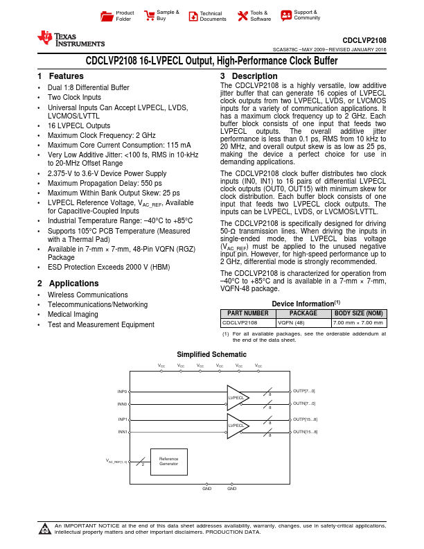
The CDCLVP2108 is a highly versatile, low additive jitter buffer that can generate 16 copies of LVPECL clock outputs from two LVPECL, LVDS, or LV
CMOS inputs for a variety of communication applications. It has a maximum clock frequency up to 2 GHz. Each buffer block consists of one input that feeds two LVPECL outputs. The overall additive jitter performance is less than 0.1 ps, RMS from 10 kHz to 20 MHz, and overall output skew is as low as 25 ps, making the device a pe...