www.ti.com
CDCM1804
SCAS697E – JULY 2003 – REVISED MAY 2005
1:3 LVPECL CLOCK BUFFER + ADDITIONAL LVCMOS OUTPUT AND PROG...
www.ti.com
CDCM1804
SCAS697E – JULY 2003 – REVISED MAY 2005
1:3 LVPECL CLOCK BUFFER + ADDITIONAL LV
CMOS OUTPUT AND PROGRAMMABLE DIVIDER
FEATURES
Distributes One Differential Clock Input to Three LVPECL Differential Clock Outputs and One LV
CMOS Single-Ended Output
Programmable Output Divider for Two LVPECL Outputs and LV
CMOS Output
Low-Output Skew 15 ps (Typical) for Clock-Distribution Applications for LVPECL Outputs; 1.6-ns Output Skew Between LV
CMOS and LVPECL Transitions Minimizing Noise
VCC Range 3 V–3.6 V Signaling Rate Up to 800-MHz LVPECL and
200-MHz LV
CMOS
Differential Input Stage for Wide Common-Mode Range
Provides VBB Bias
Voltage Output for Single-Ended Input Signals
Receiver Input Threshold ±75 mV
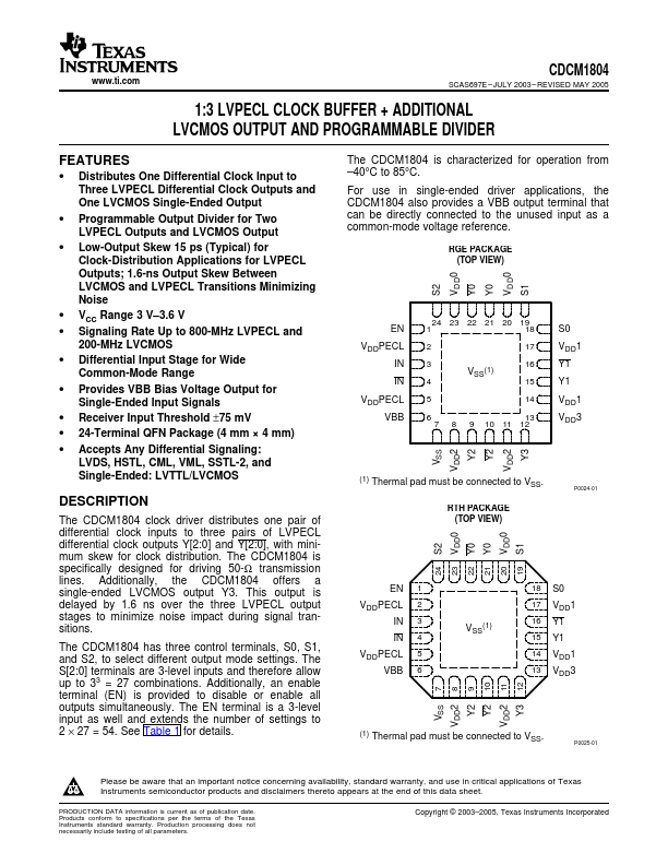
24-Terminal QFN Package (4 mm × 4 mm)
Accepts Any Differential Signaling: LVDS, HSTL, CML, VML, SSTL-2, and Single-Ended: LVTTL/LV
CMOS
DESCRIPTION
The CDCM1804 clock driver distributes one pair of differential clock inputs to three pairs of LVPECL differential clock outputs Y[2:0] and Y[2:0], with minimum skew for clock distribution. The CDCM1804 is specifically designed for driving 50-Ω transmission lines. Additionally, the CDCM1804 offers a single-ended LV
CMOS output Y3. This output is delayed by 1.6 ns over the three LVPECL output stages to minimize noise impact during signal transitions.
The CDCM1804 has three control terminals, S0, S1, and S2, to select different output mode settings. The S[2:0] terminals are 3-level inputs and therefore allow u...