Product Folder
Order Now
Technical Documents
Tools & Software
Support & Community
Reference Design
CDCM7005
SCAS79...
Product Folder
Order Now
Technical Documents
Tools & Software
Support & Community
Reference Design
CDCM7005
SCAS793G – JUNE 2005 – REVISED AUGUST 2017
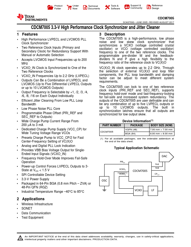
CDCM7005 3.3-V High Performance Clock Synchronizer and Jitter Cleaner
1 Features
1 High Performance LVPECL and LV
CMOS PLL Clock Synchronizer
Two Reference Clock Inputs (Primary and Secondary Clock) for Redundancy Support With Manual or Automatic Selection
Accepts LV
CMOS Input Frequencies up to 200 MHz
VCXO_IN Clock is Synchronized to One of the Two Reference Clocks
VCXO_IN Frequencies Up to 2.2 GHz (LVPECL) Outputs Can Be a Combination of LVPECL and
LV
CMOS (Up to Five Differential LVPECL Outputs or up to 10 LV
CMOS Outputs) Output Frequency is Selectable by ×1, /2, /3, /4, /6, /8, /16 on Each Output Individually Efficient Jitter Cleaning From Low PLL Loop Bandwidth Low Phase Noise PLL Core Programmable Phase Offset (PRI_REF and SEC_REF to Outputs) Wide Charge Pump Current Range From 200 μA to 3 mA Dedicated Charge Pump Supply (VCC_CP) for Wide Tuning
Voltage Range VCOs Presets Charge Pump to VCC_CP/2 for Fast Center-Frequency Setting of VC(X)O Analog and Digital PLL Lock Indication Provides VBB Bias
Voltage Output for SingleEnded Input Signals (VCXO_IN) Frequency Hold-Over Mode Improves Fail-Safe Operation Power-up Control Forces LVPECL Outputs to 3State at VCC < 1.5 V SPI Controllable Device Setting 3.3-V Power Supply Packaged in 64-Pin BGA (0.8 mm Pitch – ZVA) or 48-Pin QFN (RGZ) ...