Product Folder
Sample & Buy
Technical Documents
Tools & Software
Support & Community
Reference Design
CDCM9102
SCA...
Product Folder
Sample & Buy
Technical Documents
Tools & Software
Support & Community
Reference Design
CDCM9102
SCAS922A – FEBRUARY 2012 – REVISED APRIL 2016
CDCM9102 Low-Noise Two-Channel 100-MHz Clock Generator
1 Features
1 Integrated Low-Noise Clock Generator Including PLL, VCO, and Loop Filter
Two Low-Noise 100-MHz Clocks (LVPECL, LVDS, or pair of LV
CMOS) – Support for HCSL Signaling Levels (AC-Coupled) – Typical Period Jitter: 21 ps pk-pk – Typical Random Jitter: 510 fs RMS – Output Type Set by Pins
Bonus Single-Ended 25-MHz Output Integrated Crystal Oscillator Input Accepts
25-MHz Crystal Output Enable Pin Shuts Off Device and Outputs 5-mm × 5-mm 32-Pin VQFN Package ESD Protection Exceeds 2000 V HBM, 500 V
CDM Industrial Temperature Range (–40°C to 85°C) 3.3-V Power Supply
2 Applications
Reference Clock Generation for PCI Express Gen 1, Gen 2, and Gen 3
General-Purpose Clocking
3 Description
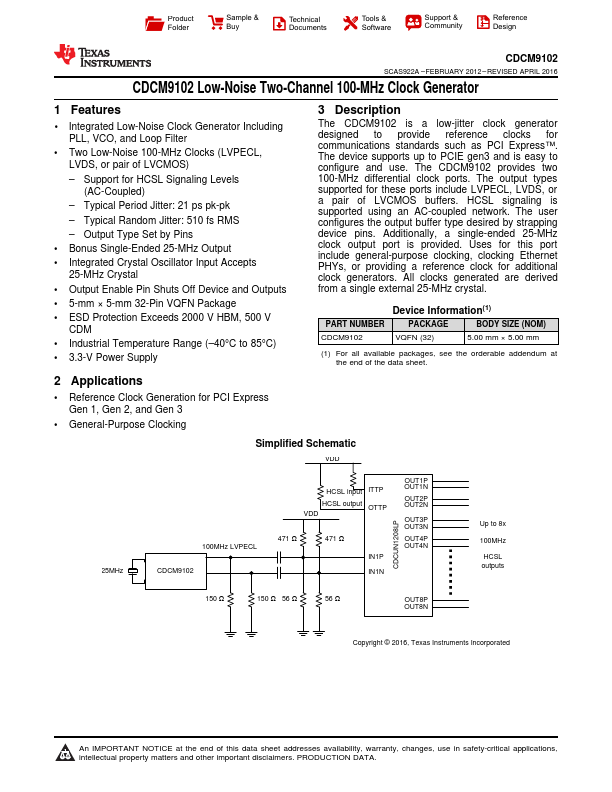
The CDCM9102 is a low-jitter clock generator designed to provide reference clocks for communications standards such as PCI Express™. The device supports up to PCIE gen3 and is easy to configure and use. The CDCM9102 provides two 100-MHz differential clock ports. The output types supported for these ports include LVPECL, LVDS, or a pair of LV
CMOS buffers. HCSL signaling is supported using an AC-coupled network. The user configures the output buffer type desired by strapping device pins. Additionally, a single-ended 25-MHz clock output port is provided. Use...