CDCS501
www.ti.com........................................................................................................
CDCS501
www.ti.com..................................................................................................................................................................................................... SCAS874 – APRIL 2009
SSC Clock Generator/Buffer
FEATURES
1
Part of a Family of Easy to use Clock Generator Devices With Optional SSC
SSC Capable Clock Generator / Buffer SSC Controllable via 3 External Pins
– ±0% to ±1.5% Center Spread 1 External Control Pin for SSC ON / OFF
Selection 40 MHz to 108 MHz Single-Ended LV
CMOS
Input Single 3.3V Device Power Supply Wide Temperature Range – 40°C to 85°C Low Space Consumption by 8 Pin TSSOP
Package
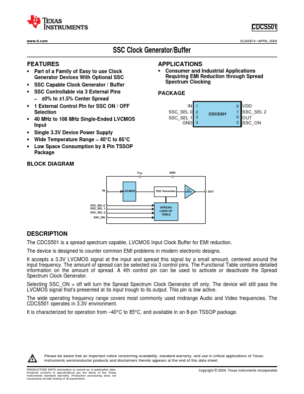
BLOCK DIAGRAM
V DD
APPLICATIONS
Consumer and Industrial Applications Requiring EMI Reduction through Spread Spectrum Clocking
PACKAGE
IN 1 SSC_SEL 0 2 SSC_SEL 1 3
GND 4
CDCS501
8 VDD 7 SSC_SEL 2 6 OUT 5 SSC_ON
GND
IN
SSC_SEL 0 SSC_SEL 1 SSC_SEL 2
SSC_ON
LV
CMOS
SSC Generator
LV
CMOS
SPREAD LOOK-UP
TABLE
OUT
DESCRIPTION
The CDCS501 is a spread spectrum capable, LV
CMOS Input Clock Buffer for EMI reduction.
The device is designed to counter common EMI problems in modern electronic designs.
It accepts a 3.3V LV
CMOS signal at the input and spread this signal by a small amount, centered around the input frequency. The amount of spread can be selected via 3 control pins. The Functional Table contains detailed information on the amount of spread. A 4th control pin can be used to activate or deactivate the...