200-MHz General-Purpose Clock Buffer
Product Folder
Order Now
Technical Documents
Tools & Software
Support & Community
CDCV304
SCAS643I – SEPTEMBER 2000...
Description
Product Folder
Order Now
Technical Documents
Tools & Software
Support & Community
CDCV304
SCAS643I – SEPTEMBER 2000 – REVISED OCTOBER 2017
CDCV304 200-MHz General-Purpose Clock Buffer, PCI-X Compliant
1 Features
1 General-Purpose and PCI-X 1:4 Clock Buffer Operating Frequency
– 0 MHz to 200 MHz General-Purpose Low Output Skew: <100 ps Distributes One Clock Input to One Bank of Four
Outputs Output Enable Control that Drives Outputs Low
when OE is Low Operates from Single 3.3-V Supply or 2.5-V
Supply PCI-X Compliant 8-Pin TSSOP Package
2 Description
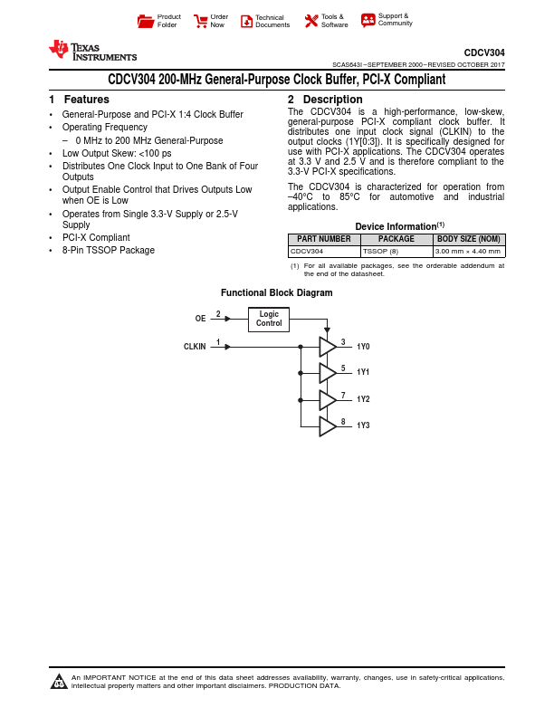
The CDCV304 is a high-performance, low-skew, general-purpose PCI-X compliant clock buffer. It distributes one input clock signal (CLKIN) to the output clocks (1Y[0:3]). It is specifically designed for use with PCI-X applications. The CDCV304 operates at 3.3 V and 2.5 V and is therefore compliant to the 3.3-V PCI-X specifications.
The CDCV304 is characterized for operation from –40°C to 85°C for automotive and industrial applications.
Device Information(1)
PART NUMBER
PACKAGE
BODY SIZE (NOM)
CDCV304
TSSOP (8)
3.00 mm × 4.40 mm
(1) For all available packages, see the orderable addendum at the end of the datasheet.
Functional Block Diagram
OE 2 CLKIN 1
Logic Control
3 1Y0
5 1Y1
7 1Y2
8 1Y3
1
An IMPORTANT NOTICE at the end of this data sheet addresses availability, warranty, changes, use in safety-critical applications, intellectual property matters and other important disclaimers. PRODUCTION DATA.
...
Similar Datasheet