CDCVF111 1:9 DIFFERENTIAL LVPECL CLOCK DRIVER
SCAS670B – SEPTEMBER 2001 – REVISED JUNE 2002
D Low-Output Skew for Cloc...
CDCVF111 1:9 DIFFERENTIAL LVPECL CLOCK DRIVER
SCAS670B – SEPTEMBER 2001 – REVISED JUNE 2002
D Low-Output Skew for Clock-Distribution
Applications
D Differential Low-
Voltage Pseudo-ECL
(LVPECL) Compatible Inputs and Outputs
D Distributes Differential Clock Inputs to Nine
Differential Clock Outputs
D Output Reference
Voltage (VREF ) Allows
Distribution From a Single-Ended Clock Input
D Packaged In a 28-Pin Plastic Chip Carrier
description
The differential LVPECL clock-driver circuit distributes one pair of differential LVPECL clock inputs (CLKIN, CLKIN) to nine pairs of differential clock (Y, Y) outputs with minimum skew for clock distribution. It is specifically designed for driving 50-Ω transmission lines.
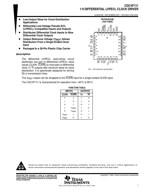
FN PACKAGE (TOP VIEW)
NC VREF CLKIN VCC CLKIN NC GND
Y8 Y8 Y7 VCC Y7 Y6 Y6
4 3 2 1 28 27 26
5
25
6
24
7
23
8
22
9
21
10
20
11
19
12 13 14 15 16 17 18
Y0 Y0 Y1 VCC Y1 Y2 Y2
Y5 Y5 Y4 VCC Y4 Y3 Y3
NC – No internal connection
The VREF output can be strapped to the CLKIN input for a single-ended CLKIN input. The CDCVF111 is characterized for operation from –40°C to 85°C.
FUNCTION TABLE
INPUTS
OUTPUTS
CLKIN CLKIN Yn Yn
X
X
L
H
L
H
L
H
H
L
H
L
L
VREF
L
H
H
VREF H
L
VREF
L
H
L
VREF
H
L
H
Please be aware that an important notice concerning availability, standard warranty, and use in critical applications of Texas Instruments semiconductor products and disclaimers thereto appears at the end of this data sheet.
PRODUCTION DATA ...