2.5-V TO 3.3-V HIGH-PERFORMANCE CLOCK BUFFER
CDCVF2310-EP
www.ti.com
SCAS934 – DECEMBER 2012
2.5-V TO 3.3-V HIGH-PERFORMANCE CLOCK BUFFER
Check for Samples: CDCVF...
Description
CDCVF2310-EP
www.ti.com
SCAS934 – DECEMBER 2012
2.5-V TO 3.3-V HIGH-PERFORMANCE CLOCK BUFFER
Check for Samples: CDCVF2310-EP
FEATURES
1
High-Performance 1:10 Clock Driver Operates up to 200 MHz at VDD 3.3 V Pin-to-Pin Skew < 100 ps at VDD 3.3 V VDD Range: 2.3 V to 3.6 V Output Enable Glitch Suppression Distributes One Clock Input to Two Banks of
Five Outputs 25-Ω On-Chip Series Damping Resistors Packaged in 24-Pin TSSOP
APPLICATIONS
General-Purpose Applications
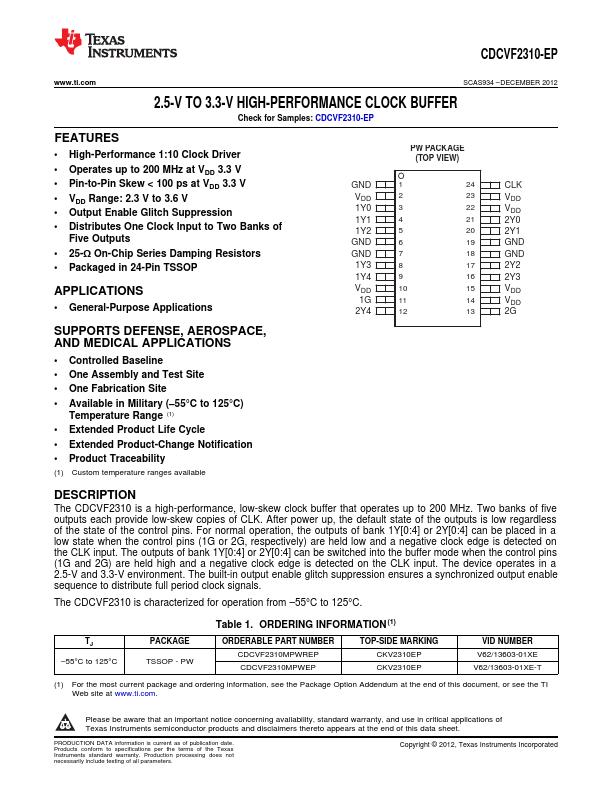
GND VDD 1Y0 1Y1 1Y2 GND GND 1Y3 1Y4 VDD
1G 2Y4
PW PACKAGE (TOP VIEW)
1
24
2
23
3
22
4
21
5
20
6
19
7
18
8
17
9
16
10
15
11
14
12
13
CLK VDD VDD 2Y0 2Y1 GND GND 2Y2 2Y3 VDD VDD 2G
SUPPORTS DEFENSE, AEROSPACE, AND MEDICAL APPLICATIONS
Controlled Baseline One Assembly and Test Site One Fabrication Site Available in Military (–55°C to 125°C)
Temperature Range (1) Extended Product Life Cycle Extended Product-Change Notification Product Traceability
(1) Custom temperature ranges available
DESCRIPTION
The CDCVF2310 is a high-performance, low-skew clock buffer that operates up to 200 MHz. Two banks of five outputs each provide low-skew copies of CLK. After power up, the default state of the outputs is low regardless of the state of the control pins. For normal operation, the outputs of bank 1Y[0:4] or 2Y[0:4] can be placed in a low state when the control pins (1G or 2G, respectively) are held low and a negative clock edge is detected on the CLK input. The outputs...
Similar Datasheet