3.3-V CLOCK PHASE-LOCKED LOOP CLOCK DRIVER
CDCVF2505-Q1
www.ti.com...................................................................................................
Description
CDCVF2505-Q1
www.ti.com........................................................................................................................................................................................... SCAS867 – DECEMBER 2008
3.3-V CLOCK PHASE-LOCKED LOOP CLOCK DRIVER
FEATURES
1
Qualified for Automotive Applications Phase-Locked Loop Clock Driver for
Synchronous DRAM and General-Purpose Applications
Spread-Spectrum Clock Compatible Operating Frequency: 24 MHz to 200 MHz Low Jitter (Cycle-to-Cycle): <150 ps Over the
Range 66 MHz to 200 MHz
Distributes One Clock Input to One Bank of Five Outputs (CLKOUT Is Used to Tune the Input-Output Delay)
Three-States Outputs When There Is No Input Clock
Operates From Single 3.3-V Supply Available in 8-Pin SOIC Package
Consumes Less Than 100 µA (Typically) in Power Down Mode
Internal Feedback Loop Is Used to Synchronize the Outputs to the Input Clock
25-Ω On-Chip Series Damping Resistors Integrated RC PLL Loop Filter Eliminates the
Need for External Components
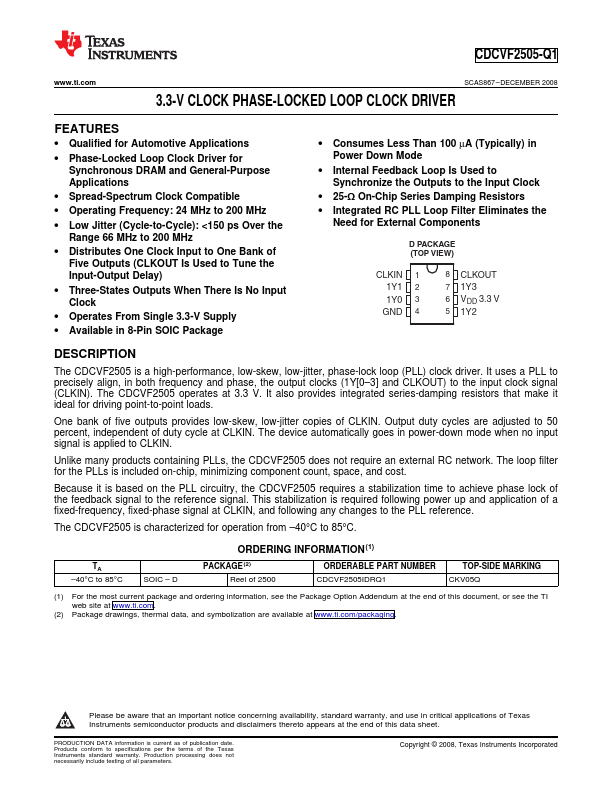
D PACKAGE (TOP VIEW)
CLKIN 1 1Y1 2 1Y0 3 GND 4
8 CLKOUT 7 1Y3 6 VDD 3.3 V 5 1Y2
DESCRIPTION
The CDCVF2505 is a high-performance, low-skew, low-jitter, phase-lock loop (PLL) clock driver. It uses a PLL to precisely align, in both frequency and phase, the output clocks (1Y[0–3] and CLKOUT) to the input clock signal (CLKIN). The CDCVF2505 operates at 3.3 V. It also provides integrated series-damping resistors that make it ideal for driving point-...
Similar Datasheet