2.5-V TO 3.3-V HIGH-PERFORMANCE CLOCK BUFFER
www.ti.com
CDCVF310
SCAS771B – AUGUST 2004 – REVISED JANUARY 2008
2.5-V TO 3.3-V HIGH-PERFORMANCE CLOCK BUFFER
FEATURE...
Description
www.ti.com
CDCVF310
SCAS771B – AUGUST 2004 – REVISED JANUARY 2008
2.5-V TO 3.3-V HIGH-PERFORMANCE CLOCK BUFFER
FEATURES
1
High-Performance 1:10 Clock Driver Pin-to-Pin Skew < 100 ps at VDD 3.3 V VDD Range = 2.3 V to 3.6 V Input Clock Up To 200 MHz (See Figure 7) Operating Temperature Range –40°C to 85°C Output Enable Glitch Suppression Distributes One Clock Input to Two Banks of
Five Outputs Packaged in 24-Pin TSSOP Pin-to-Pin Compatible to the CDCVF2310,
Except the R = 22-Ω Series Damping Resistors at Yn
APPLICATIONS
General-Purpose Applications
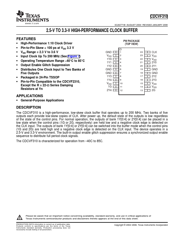
GND VDD 1Y0 1Y1 1Y2 GND GND 1Y3 1Y4 VDD
1G 2Y4
PW PACKAGE (TOP VIEW)
1
24
2
23
3
22
4
21
5
20
6
19
7
18
8
17
9
16
10
15
11
14
12
13
CLK VDD VDD 2Y0 2Y1 GND GND 2Y2 2Y3 VDD VDD 2G
DESCRIPTION
The CDCVF310 is a high-performance, low-skew clock buffer that operates up to 200 MHz. Two banks of five outputs each provide low-skew copies of CLK. After power up, the default state of the outputs is low regardless of the state of the control pins. For normal operation, the outputs of bank 1Y[0:4] or 2Y[0:4] can be placed in a low state when the control pins (1G or 2G, respectively) are held low and a negative clock edge is detected on the CLK input. The outputs of bank 1Y[0:4] or 2Y[0:4] can be switched into the buffer mode when the control pins (1G and 2G) are held high and a negative clock edge is detected on the CLK input. The device operates in a 2.5-V and 3.3-V environment. The built-in ou...
Similar Datasheet