CED4301/CEU4301
P-Channel Enhancement Mode Field Effect Transistor
FEATURES
-40V, -20A, RDS(ON) = 42mΩ @VGS = -10V. RDS...
CED4301/CEU4301
P-Channel Enhancement Mode Field Effect Transistor
FEATURES
-40V, -20A, RDS(ON) = 42mΩ @VGS = -10V. RDS(ON) = 65mΩ @VGS = -4.5V.
Super high dense cell design for extremely low RDS(ON). High power and current handing capability. Lead free product is acquired. TO-251 & TO-252 package.
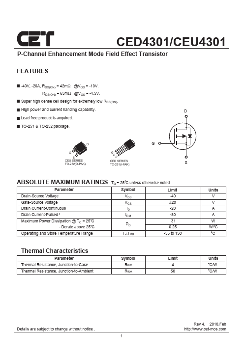
D
D
G S
CEU SERIES TO-252(D-PAK)
G DS
CED SERIES TO-251(I-PAK)
G
S
ABSOLUTE MAXIMUM RATINGS Tc = 25 C unless otherwise noted
Parameter
Symbol
Limit
Drain-Source
Voltage Gate-Source
Voltage Drain Current-Continuous Drain Current-Pulsed a Maximum Power Dissipation @ TC = 25 C
- Derate above 25 C
VDS VGS ID IDM
PD
-40
±20
-20 -80 31 0.25
Operating and Store Temperature Range
TJ,Tstg
-55 to 150
Thermal Characteristics
Parameter Thermal Resistance, Junction-to-Case Thermal Resistance, Junction-to-Ambient
Symbol RθJC RθJA
Limit 4 50
Units V V A A W
W/ C C
Units C/W C/W
Details are subject to change without notice .
1
Rev 4. 2010.Feb http://www.cet-mos.com
CED4301/CEU4301
Electrical Characteristics TA = 25 C unless otherwise noted
Parameter
Symbol
Test Condition
Off Characteristics
Drain-Source Breakdown
Voltage Zero Gate
Voltage Drain Current Gate Body Leakage Current, Forward Gate Body Leakage Current, Reverse On Characteristics c
BVDSS IDSS IGSSF IGSSR
VGS = 0V, ID = -250µA VDS = -32V, VGS = 0V VGS = 20V, VDS = 0V VGS = -20V, VDS = 0V
Gate Threshold
Voltage Static Drain-Source On-Resistance Dynamic Characteristics d Forward Transconductance Input Capaci...