CEEF02N65G
N-Channel Enhancement Mode Field Effect Transistor
FEATURES
650V, 2.0A, RDS(ON) = 5.0Ω @VGS = 10V. Super hig...
CEEF02N65G
N-Channel Enhancement Mode Field Effect Transistor
FEATURES
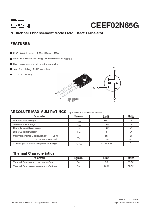
650V, 2.0A, RDS(ON) = 5.0Ω @VGS = 10V. Super high dense cell design for extremely low RDS(ON). High power and current handing capability. Lead-free plating ; RoHS compliant. TO-126F package.
D
G D S
CEE SERIES TO-126F
G
S
ABSOLUTE MAXIMUM RATINGS Tc = 25 C unless otherwise noted
Parameter
Symbol
Limit
Drain-Source
Voltage Gate-Source
Voltage Drain Current-Continuous Drain Current-Pulsed a Maximum Power Dissipation @ TC = 25 C
- Derate above 25 C
VDS VGS ID IDM
PD
650
±30
2d 8 56 0.44
Operating and Store Temperature Range
TJ,Tstg
-55 to 150
Thermal Characteristics
Parameter Thermal Resistance, Junction-to-Case Thermal Resistance, Junction-to-Ambient
Symbol RθJC RθJA
Limit 2.3 62.5
Units V V A A W
W/ C C
Units C/W C/W
Details are subject to change without notice .
1
Rev 1. 2012.Mar http://www.cetsemi.com
CEEF02N65G
Electrical Characteristics Tc = 25 C unless otherwise noted
Parameter
Sy...