CEP02N6G/CEB02N6G CEF02N6G
N-Channel Enhancement Mode Field Effect Transistor
FEATURES
Type CEP02N6G CEB02N6G CEF02N6G...
CEP02N6G/CEB02N6G CEF02N6G
N-Channel Enhancement Mode Field Effect Transistor
FEATURES
Type CEP02N6G CEB02N6G CEF02N6G
VDSS 600V 600V
600V
RDS(ON) 5Ω 5Ω
5Ω
ID 2.2A 2.2A 2.2A d
@VGS 10V 10V
10V
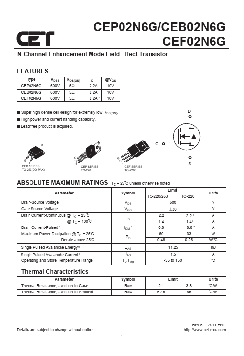
Super high dense cell design for extremely low RDS(ON). High power and current handing capability. Lead free product is acquired.
D
DG
GS
CEB SERIES TO-263(DD-PAK)
G D S
CEP SERIES TO-220
G
D S CEF SERIES
TO-220F
S
ABSOLUTE MAXIMUM RATINGS
Parameter
Drain-Source
Voltage Gate-Source
Voltage Drain Current-Continuous @ TC = 25 C
@ TC = 100 C Drain Current-Pulsed a Maximum Power Dissipation @ TC = 25 C
- Derate above 25 C
Tc = 25 C unless otherwise noted
Symbol
Limit TO-220/263
VDS 600
VGS ±30
ID
2.2 1.4
IDM e
8.8
60 PD 0.48
TO-220F
2.2 d 1.4d 8.8 d 33 0.26
Single Pulsed Avalanche Energy g
Single Pulsed Avalanche Current g Operating and Store Temperature Range
EAS IAS TJ,Tstg
11.25 1.5
-55 to 150
Thermal Characteristics
Parameter Thermal Resistance, Junction-to-Case Thermal Resistance, Junction-to-Ambient
Symbol RθJC RθJA
Limit 2.1 62.5
3.8 65
Units
V V A A A W W/ C mJ A C
Units C/W C/W
Details are subject to change without notice .
1
Rev 5. 2011.Feb http://www.cet-mos.com
CEP02N6G/CEB02N6G CEF02N6G
Electrical Characteristics Tc = 25 C unless otherwise noted
Parameter
Symbol
Test Condition
Min Typ Max Units
Off Characteristics
Drain-Source Breakdown
Voltage Zero Gate
Voltage Drain Current Gate Body Leakage Current, Forward Gate Body Leakage Current...