CEF06N5
Oct. 2002
N-Channel Logic Level Enhancement Mode Field Effect Transistor
FEATURES
500V , 4.5A , RDS(ON)=1Ω @VGS...
CEF06N5
Oct. 2002
N-Channel Logic Level Enhancement Mode Field Effect Transistor
FEATURES
500V , 4.5A , RDS(ON)=1Ω @VGS=10V.
6 Super high dense cell design for extremely low RDS(ON).
High power and current handling capability. TO-220F full-pak for through hole
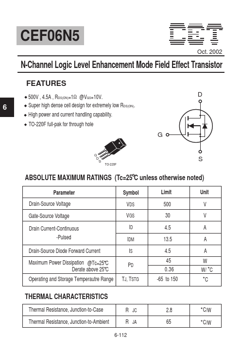
G
D
G
D S TO-220F
S
ABSOLUTE MAXIMUM RATINGS (Tc=25 C unless otherwise noted)
Parameter
Symbol
Drain-Source
Voltage
VDS
Gate-Source
Voltage
VGS
Drain Current-Continuous -Pulsed
ID IDM
Drain-Source Diode Forward Current
IS
Maximum Power Dissipation @Tc=25 C Derate above 25 C
Operating and Storage Temperautre Range
PD TJ, TSTG
Limit 500 30 4.5 13.5 4.5 45 0.36 -65 to 150
Unit V V
A A A W W/ C C
THERMAL CHARACTERISTICS
Thermal Resistance, Junction-to-Case Thermal Resistance, Junction-to-Ambient
R JC R JA
2.8 65
C/W C/W
6-112
CEF06N5
ELECTRICAL CHARACTERISTICS (TC=25 C unless otherwise noted)
Parameter
Symbol
a
DRAIN-SOURCE AVALANCHE RATING
Single Pulse Drain-Source Avalanche Energy
EAS
Maximum Dra...