Small Signal Transistor
PROCESS CP337V
Small Signal Transistor
NPN - Saturated Switch Transistor Chip
PROCESS DETAILS Process Die Size Die Thic...
Description
PROCESS CP337V
Small Signal Transistor
NPN - Saturated Switch Transistor Chip
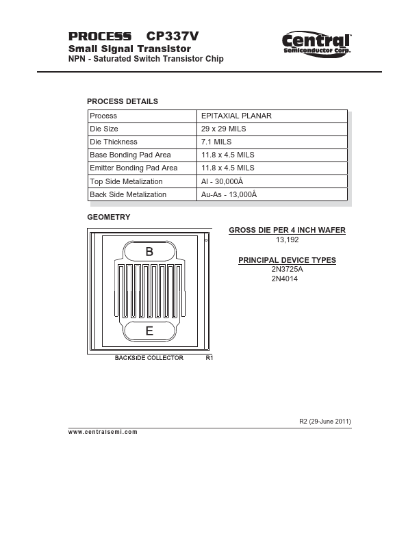
PROCESS DETAILS Process Die Size Die Thickness Base Bonding Pad Area Emitter Bonding Pad Area Top Side Metalization Back Side Metalization
GEOMETRY
EPITAXIAL PLANAR 29 x 29 MILS 7.1 MILS 11.8 x 4.5 MILS 11.8 x 4.5 MILS Al - 30,000Å Au-As - 13,000Å
GROSS DIE PER 4 INCH WAFER 13,192
PRINCIPAL DEVICE TYPES 2N3725A 2N4014
w w w. c e n t r a l s e m i . c o m
R2 (29-June 2011)
PROCESS CP337V
Typical Electrical Characteristics
w w w. c e n t r a l s e m i . c o m
R2 (29-June 2011)
BARE DIE PACKING OPTIONS
BARE DIE IN TRAY (WAFFLE) PACK CT: �Singulated die in tray (waffle) pack.
(example: CP211-PART NUMBER-CT)
CM: �Singulated die in tray (waffle) pack 100% visually inspected as per MIL-STD-750, (method 2072 transistors, method 2073 diodes).
(example: CP211-PART NUMBER-CM)
UNSAWN WAFER WN: �Full wafer, unsawn, 100% tested with reject die inked.
(example: CP211-PART NUMBER-WN)
SAWN WAFER ON PLASTIC RING WR: �Full wafer, sawn and mounted on plastic ring, 100% tested with reject die inked.
(example: CP211-PART NUMBER-WR)
Please note: Sawn Wafer on Metal Frame (WS) is possible as a special order. Please contact your Central Sales Representative at 631-435-1110.
Visit the Central website for a complete listing of specifications: www.centralsemi.com/bdspecs
w w w. c e n t r a l s e m i . c o m
R2 (3-April 2017)
OUTSTANDING SUPPORT AND SUPERIOR SERVICES
PRODUCT SUPPORT
Central’s operations team provi...
Similar Datasheet