Product Folder
Order Now
Technical Documents
Tools & Software
Support & Community
CSD13202Q2
SLPS313A – SEPTEMBER 2...
Product Folder
Order Now
Technical Documents
Tools & Software
Support & Community
CSD13202Q2
SLPS313A – SEPTEMBER 2013 – REVISED JANUARY 2018
CSD13202Q2 12-V N-Channel NexFET™ Power
MOSFETs
1 Features
1 Ultra-Low Qg and Qgd Low Thermal Resistance Avalanche Rated Lead-Free Terminal Plating RoHS Compliant Halogen Free SON 2-mm × 2-mm Plastic Package
Product Summary
TA = 25°C
VDS
Drain-to-Source
Voltage
Qg
Gate Charge Total (4.5 V)
Qgd
Gate Charge Gate-to-Drain
RDS(on) Drain-to-Source On-Resistance
VGS(th) Threshold
Voltage
TYPICAL VAUE
12
5.1
0.76
VGS = 2.5 V
9.1
VGS = 4.5 V
7.5
0.8
UNIT V nC nC
mΩ
V
2 Applications
Optimized for Load Switch Applications Storage, Tablets, and Handheld Devices Optimized for Control FET Applications Point of Load Synchronous Buck Converters
3 Description
This 12-V, 7.5-mΩ NexFET™ power
MOSFET has been designed to minimize losses in power conversion and load management applications. The SON 2 × 2 offers excellent thermal performance for the size of the package.
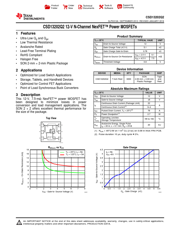
Top View
D1 D
D2
6D 5D
G3
S
4S
DEVICE CSD13202Q2
Device Information
MEDIA
QTY
PACKAGE
7-Inch Reel
3000
SON 2.00-mm × 2.00-mm
Plastic Package
SHIP
Tape and Reel
Absolute Maximum Ratings
TA = 25°C
VDS Drain-to-Source
Voltage
VGS Gate-to-Source
Voltage
Continuous Drain Current (Package Limit)
ID
Continuous Drain Current(1)
IDM Pulsed Drain Current, TA = 25°C(2)
PD
Power Dissipation(1)
TJ, Operating Junction, TSTG Storage T...