CSD16412Q5A
www.ti.com
SLPS207A – AUGUST 2009 – REVISED SEPTEMBER 2010
N-Channel NexFET™ Power MOSFETs
Check for Sampl...
CSD16412Q5A
www.ti.com
SLPS207A – AUGUST 2009 – REVISED SEPTEMBER 2010
N-Channel NexFET™ Power
MOSFETs
Check for Samples: CSD16412Q5A
FEATURES
1
2 Ultra Low Qg and Qgd Low Thermal Resistance Avalanche Rated Pb Free Terminal Plating RoHS Compliant Halogen Free SON 5mm x 6mm Plastic Package
APPLICATIONS
Point-of-Load Synchronous Buck Converter for Applications in Networking, Telecom and Computing Systems
Optimized for Control FET Applications
DESCRIPTION
The NexFET™ power
MOSFET has been designed to minimize losses in power conversion applications.
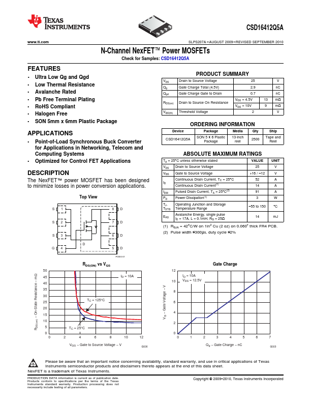
Top View
S1
8D
S2
7D
S3
6D
VDS Qg Qgd
RDS(on)
VGS(th)
PRODUCT SUMMARY
Drain to Source
Voltage
25
Gate Charge Total (4.5V)
2.9
Gate Charge Gate to Drain
0.7
Drain to Source On Resistance Threshold
Voltage
VGS = 4.5V VGS = 10V
2
V nC nC 13 mΩ 9 mΩ V
ORDERING INFORMATION
Device
Package
Media
Qty
CSD16412Q5A
SON 5 × 6 Plastic Package
13-inch reel
2500
Ship
Tape and Reel
ABSOLUTE MAXIMUM RATINGS
TA = 25°C unless otherwise stated
VDS Drain to Source
Voltage
VGS Gate to Source
Voltage
ID
Continuous Drain Current, TC = 25°C Continuous Drain Current(1)
IDM Pulsed Drain Current, TA = 25°C(2)
PD
Power Dissipation(1)
TJ, Operating Junction and Storage TSTG Temperature Range
EAS
Avalanche Energy, single pulse ID = 17A, L = 0.1mH, RG = 25Ω
VALUE 25
+16 / –12 52 14 91 3
UNIT V V A A A W
–55 to 150 °C
14
mJ
(1) RθJA = 42°C/W on 1in2 Cu (2 oz) on 0.060" thick FR4 PCB. (2) Pulse width ≤3...